Terasic Cyclone IV Deo-Nano Starter Kit for Cyclone IV P0082
- RS 제품 번호:
- 768-9039
- 제조사 부품 번호:
- P0082
- 제조업체:
- Terasic

대량 구매 할인 기용 가능
View bulk pricing optionsSubtotal (1 unit)*
₩287,700.00
재고있음
- 추가로 2026년 7월 13일 부터 32 개 단위 배송
- 추가로 2026년 9월 03일 부터 18 개 단위 배송
- 추가로 2026년 11월 05일 부터 18 개 단위 배송
더 자세한 내용이 필요하신가요? 필요한 수량을 입력하고 '배송일 확인'을 클릭하면 더 많은 재고 및 배송 세부정보를 확인하실 수 있습니다.
수량 | 한팩당 |
|---|---|
| 1 - 4 | ₩287,700.00 |
| 5 + | ₩276,180.00 |
* 참고 가격: 실제 구매가격과 다를 수 있습니다
- RS 제품 번호:
- 768-9039
- 제조사 부품 번호:
- P0082
- 제조업체:
- Terasic
사양
참조 문서
제정법과 컴플라이언스
제품 세부 사항
제품 정보를 선택해 유사 제품을 찾기
모두 선택 | 제품 정보 | 값 |
|---|---|---|
| 브랜드 | Terasic | |
| Kit Classification | Starter Kit | |
| Product Type | Communication & Wireless Development Tool | |
| For Use With | Cyclone IV | |
| Kit Name | Cyclone IV Deo-Nano | |
| Interface Type | USB | |
| Standards/Approvals | RoHS | |
| 모두 선택 | ||
|---|---|---|
브랜드 Terasic | ||
Kit Classification Starter Kit | ||
Product Type Communication & Wireless Development Tool | ||
For Use With Cyclone IV | ||
Kit Name Cyclone IV Deo-Nano | ||
Interface Type USB | ||
Standards/Approvals RoHS | ||
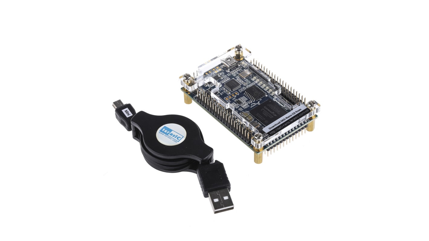
Cyclone IV DE0-Nano Starter Kit
The DE0-Nano board introduces a compact-sized FPGA development platform suited for prototyping circuit designs such as robots and "portable" projects. The board is designed, to be used in the simplest possible implementation targeting the Cyclone IV device with up to 22320 LEs.
The advantages of the DE0-Nano board include its size, weight and its ability to be reconfigured without carrying superfluous hardware. These features set it apart from other general purpose development boards.
Parallax has made all the design files for their 8-core Propeller microcontroller Open Source. Details of how to program the DE0-Nano as a Propeller together with all the necessary files can be found at:
http://www.parallax.com/microcontrollers/propeller-1-open-source
Altera Cyclone IV EP4CE22F17C6N FPGA, 22320 x Logic Elements, 594Kb memory, 66 x multipliers, 4 x PLLs, Maximum 153 x I/O pins
64 MB configuration Flash memory
50 MHz clock oscillator
32 MB SDRAM
2Kb I2C EEPROM
ADXL345 3-axis accelerometer
ADC128S022, 8-Channel, 12-bit A/D Converter, 50ksps to 200ksps
8 x green LEDs
2 x debounced push buttons
4 x dip switches
Power supply: Mini USB connector (5 V), Two GPIO header pins (5 V), 2-pin external power header (+3.6 to +5.7 V)
On-board USB-Blaster circuit for programming
Two 40-pin headers provide 72 x digital I/O pins
One 26-pin header provides 16 x digital I/O pins and 8 x analogue input pins
An FPGA is a semiconductor device consisting of a matrix of Configurable Logic Blocks (CLBs) connected through programmable interconnects. The user determines these interconnections by programming SRAM. A CLB can be simple (AND, OR gates, etc) or complex (a block of RAM). The FPGA allows changes to be made to a design even after the device is soldered into a PCB.
Supplied with
USB cable, System CD, Altera complete design suite free package, Quick Start Guide
관련된 링크들
- Terasic SDI to HSMC SDI HSMC Board Adapter Board for Stratix IV GX FPGA Development Board P0039
- Terasic GPIO to HSMC/HSTC Adapter Board for DE3, DE2 P0024
- Altera FPGA Cyclone IV 28848 Cells, 594 bit 1803 Blocks, 484-Pin FBGA
- Altera FPGA Cyclone IV GX 14400 Cells, 540000 bit 900 Blocks, 169-Pin FBGA
- Altera FPGA Cyclone IV E 6272 Cells, 6272 Gates, 276480 bit 392 Blocks, 256-Pin FBGA
- Altera FPGA Cyclone IV E 6272 Cells, 6272 Gates, 276480 bit 392 Blocks, 144-Pin EQFP
- Silicon Labs Wireless Starter Kit Radio Board ZigBee, Thread, Bluetooth Starter Kit for Wireless Starter Kit Mainboard
- Silicon Labs Wireless Starter Kit Radio Board Bluetooth Starter Kit for Wireless Starter Kit Mainboard 1.1 MHz