Terasic SDI to HSMC SDI HSMC Board Adapter Board for Stratix IV GX FPGA Development Board P0039
- RS 제품 번호:
- 768-9035
- 제조사 부품 번호:
- P0039
- 제조업체:
- Terasic

Subtotal (1 unit)*
₩1,223,000.00
일시적 품절
- 2026년 8월 31일 부터 배송
더 자세한 내용이 필요하신가요? 필요한 수량을 입력하고 '배송일 확인'을 클릭하면 더 많은 재고 및 배송 세부정보를 확인하실 수 있습니다.
수량 | 한팩당 |
|---|---|
| 1 + | ₩1,223,000.00 |
* 참고 가격: 실제 구매가격과 다를 수 있습니다
- RS 제품 번호:
- 768-9035
- 제조사 부품 번호:
- P0039
- 제조업체:
- Terasic
사양
참조 문서
제정법과 컴플라이언스
제품 세부 사항
제품 정보를 선택해 유사 제품을 찾기
모두 선택 | 제품 정보 | 값 |
|---|---|---|
| 브랜드 | Terasic | |
| Product Type | Communication & Wireless Development Tool | |
| Kit Classification | Adapter Board | |
| For Use With | Stratix IV GX FPGA Development Board | |
| Featured Device | SDI HSMC Board | |
| Kit Name | SDI to HSMC | |
| Interface Type | HSMC | |
| Standards/Approvals | AES3, SDI | |
| 모두 선택 | ||
|---|---|---|
브랜드 Terasic | ||
Product Type Communication & Wireless Development Tool | ||
Kit Classification Adapter Board | ||
For Use With Stratix IV GX FPGA Development Board | ||
Featured Device SDI HSMC Board | ||
Kit Name SDI to HSMC | ||
Interface Type HSMC | ||
Standards/Approvals AES3, SDI | ||
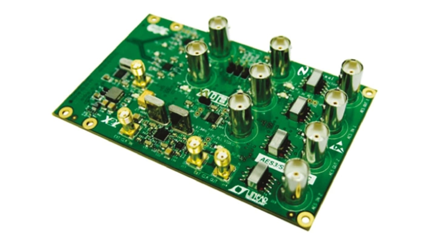
Terasic SDI HSMC Board
The Transceiver Serial Digital Interface (SDI) HSMC board provides a hardware platform for developing video broadcasting systems. It is intended to be used by customers to implement and design SDI and AES systems based on transceiver-based host boards with an HSMC interface. It can also be part of an openly sold Development Kit, or bundled with packages of software and IP cores.
2 x SDI transmit (TX) channels with SDI cable tri-speed drivers
2 x SDI receive (RX) channels with SDI cable equalizers
2 x 75Ω BNC SDI TX interfaces
2 x 75Ω BNC SDI RX interfaces
Adjustable 1.1 to 1.8V and standard 3.3V CMOS Input Signal Levels
2 x RS-422 transceivers for AES3 TX and AES3 RX channels
2 x 75Ω BNC AES3 RX interfaces
2 x 75Ω BNC AES3 TX interfaces
High frequency switching regulator for 12V to 5V power supply conversion
3 x linear regulators for 5V to 3.3V low noise power supply conversion
FDTIM analysis for power distribution network (PDN) decoupling
SDI multi-frequency VCXO femto clock video PLL
98.304MHz / 90.3168MHz / 122.88MHz / 112.896MHz voltage-controlled crystal oscillator (VCXO) based phase-locked loop (PLL)
LVPECL differential clock buffer with two differential outputs - HSMC and SMA
4 x digital audio isolation transformers
Multi-format video sync separator
HSMC connector for interface conversion, fully compatible with HSMC host boards
An FPGA is a semiconductor device consisting of a matrix of Configurable Logic Blocks (CLBs) connected through programmable interconnects. The user determines these interconnections by programming SRAM. A CLB can be simple (AND, OR gates, etc) or complex (a block of RAM). The FPGA allows changes to be made to a design even after the device is soldered into a PCB.
Supplied with
System CD ROM
관련된 링크들
- Terasic GPIO to HSMC/HSTC Adapter Board for DE3, DE2 P0024
- Digilent 410-319-1 FPGA Development Board for Makers and Hobbyists Development Board ADC1410 for DAC121S101
- Broadcom 1.9 V Red LED 1606 Surface HSMC HSMC-C120
- Digilent 410-372 Adapter for use with APSoC Development Board, FPGA
- Digilent 410-370 Cora Z7: Zynq-7000 Development Board ADC1410 for FPGA Development, ARM Development
- Broadcom 1.9 V Red LED 1606 Surface HSMC
- Altera FPGA Cyclone IV GX 14400 Cells, 540000 bit 900 Blocks, 169-Pin FBGA
- Terasic Cyclone IV Deo-Nano Starter Kit for Cyclone IV P0082