Winbond DDR2 SDRAM 128 MB Surface, 84-Pin 16 bit TFBGA
- RS 제품 번호:
- 188-2580
- 제조사 부품 번호:
- W9712G6KB25I
- 제조업체:
- Winbond

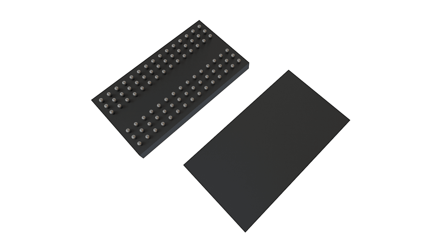
본 이미지는 참조용이오니 재확인이 필요하시면 문의해주세요.
대량 구매 할인 기용 가능
View bulk pricing optionsSubtotal (1 tray of 209 units)*
₩1,357,246.00
일시적 품절
- 2026년 12월 08일 부터 배송
더 자세한 내용이 필요하신가요? 필요한 수량을 입력하고 '배송일 확인'을 클릭하면 더 많은 재고 및 배송 세부정보를 확인하실 수 있습니다.
수량 | 한팩당 | Per Tray* |
|---|---|---|
| 209 - 209 | ₩6,494.00 | ₩1,357,204.00 |
| 418 - 627 | ₩6,364.00 | ₩1,330,076.00 |
| 836 + | ₩6,236.00 | ₩1,303,450.00 |
* 참고 가격: 실제 구매가격과 다를 수 있습니다
- RS 제품 번호:
- 188-2580
- 제조사 부품 번호:
- W9712G6KB25I
- 제조업체:
- Winbond
사양
참조 문서
제정법과 컴플라이언스
제품 세부 사항
제품 정보를 선택해 유사 제품을 찾기
모두 선택 | 제품 정보 | 값 |
|---|---|---|
| 브랜드 | Winbond | |
| Memory Size | 128MB | |
| Product Type | DDR2 SDRAM | |
| Organisation | 16M x 8 bit | |
| Data Bus Width | 16bit | |
| Address Bus Width | 15bit | |
| Number of Bits per Word | 8 | |
| Maximum Random Access Time | 0.4ns | |
| Number of Words | 16M | |
| Mount Type | Surface | |
| Package Type | TFBGA | |
| Pin Count | 84 | |
| Minimum Operating Temperature | -40°C | |
| Maximum Operating Temperature | 95°C | |
| Length | 12.6mm | |
| Series | W9712G6KB | |
| Height | 0.8mm | |
| Standards/Approvals | RoHS | |
| Width | 8.1mm | |
| Minimum Supply Voltage | 1.7V | |
| Automotive Standard | No | |
| Maximum Supply Voltage | 1.9V | |
| Supply Current | 135mA | |
| 모두 선택 | ||
|---|---|---|
브랜드 Winbond | ||
Memory Size 128MB | ||
Product Type DDR2 SDRAM | ||
Organisation 16M x 8 bit | ||
Data Bus Width 16bit | ||
Address Bus Width 15bit | ||
Number of Bits per Word 8 | ||
Maximum Random Access Time 0.4ns | ||
Number of Words 16M | ||
Mount Type Surface | ||
Package Type TFBGA | ||
Pin Count 84 | ||
Minimum Operating Temperature -40°C | ||
Maximum Operating Temperature 95°C | ||
Length 12.6mm | ||
Series W9712G6KB | ||
Height 0.8mm | ||
Standards/Approvals RoHS | ||
Width 8.1mm | ||
Minimum Supply Voltage 1.7V | ||
Automotive Standard No | ||
Maximum Supply Voltage 1.9V | ||
Supply Current 135mA | ||
The W9712G6KB is a 128M bits DDR2 SDRAM and speed involving -25, 25I and -3.
Double Data Rate architecture: two data transfers per clock cycle
CAS Latency: 3, 4, 5 and 6
Burst Length: 4 and 8
Bi-directional, differential data strobes (DQS and /DQS ) are transmitted / received with data
Edge-aligned with Read data and center-aligned with Write data
DLL aligns DQ and DQS transitions with clock
Differential clock inputs (CLK and /CLK)
Data masks (DM) for write data
Commands entered on each positive CLK edge, data and data mask are referenced to both edges of /DQS
Posted /CAS programmable additive latency supported to make command and data bus efficiency
Read Latency = Additive Latency plus CAS Latency (RL = AL + CL)
Off-Chip-Driver impedance adjustment (OCD) and On-Die-Termination (ODT) for better signal quality
Auto-precharge operation for read and write bursts
Auto Refresh and Self Refresh modes
Precharged Power Down and Active Power Down
Write Data Mask
Write Latency = Read Latency - 1 (WL = RL - 1)
Interface: SSTL_18
관련된 링크들
- Winbond DDR2 SDRAM 128 MB Surface, 84-Pin 16 bit TFBGA
- Winbond W9712G6KB25I DDR2 SDRAM 128 MB Surface, 84-Pin 16 bit TFBGA
- Winbond SDRAM 512 MB Surface, 84-Pin 16 bit VFBGA
- Winbond W9812G6KH-6I SDRAM 128 MB Surface, 54-Pin 16 bit TSOP
- Winbond W9751G6NB25I SDRAM 512 MB Surface, 84-Pin 16 bit VFBGA
- Winbond W972GG6KB25I SDRAM 2 GB Surface, 84-Pin 16 bit WBGA
- Micron MT47H32M16NF-25E:H SDRAM 512 MB Surface Mount, 84-Pin 16 bit TFBGA
- Micron MT47H32M16NF-25E IT:H SDRAM 512 MB Surface Mount, 84-Pin 16 bit TFBGA