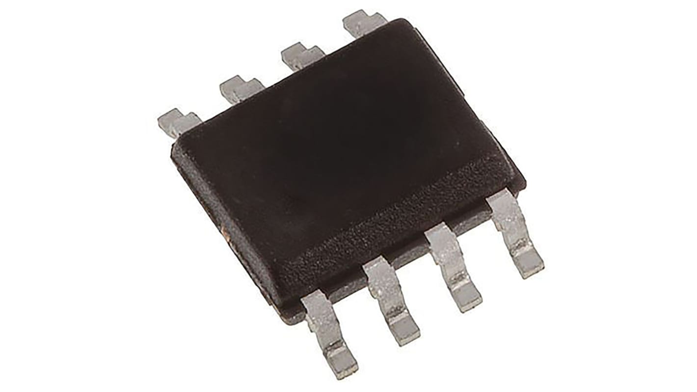
Infineon Isolated HEXFET 2 Type P, Type N-Channel MOSFET, 3.5 A, 30 V Enhancement, 8-Pin SOIC IRF9952TRPBF
- RS 제품 번호:
- 827-3934
- 제조사 부품 번호:
- IRF9952TRPBF
- 제조업체:
- Infineon

본 이미지는 참조용이오니 재확인이 필요하시면 문의해주세요.
대량 구매 할인 기용 가능
Subtotal (1 pack of 20 units)*
₩19,656.00
재고있음
- 340 개 단위 배송 준비 완료
- 추가로 2026년 4월 24일 부터 3,620 개 단위 배송
더 자세한 내용이 필요하신가요? 필요한 수량을 입력하고 '배송일 확인'을 클릭하면 더 많은 재고 및 배송 세부정보를 확인하실 수 있습니다.
수량 | 한팩당 | 한팩당* |
|---|---|---|
| 20 - 980 | ₩982.80 | ₩19,636.50 |
| 1000 + | ₩955.50 | ₩19,129.50 |
* 참고 가격: 실제 구매가격과 다를 수 있습니다
- RS 제품 번호:
- 827-3934
- 제조사 부품 번호:
- IRF9952TRPBF
- 제조업체:
- Infineon
사양
참조 문서
제정법과 컴플라이언스
제품 세부 사항
제품 정보를 선택해 유사 제품을 찾기
모두 선택 | 제품 정보 | 값 |
|---|---|---|
| 브랜드 | Infineon | |
| Channel Type | Type P, Type N | |
| Product Type | MOSFET | |
| Maximum Continuous Drain Current Id | 3.5A | |
| Maximum Drain Source Voltage Vds | 30V | |
| Package Type | SOIC | |
| Series | HEXFET | |
| Mount Type | Surface | |
| Pin Count | 8 | |
| Maximum Drain Source Resistance Rds | 400mΩ | |
| Channel Mode | Enhancement | |
| Forward Voltage Vf | 0.82V | |
| Maximum Power Dissipation Pd | 2W | |
| Minimum Operating Temperature | -55°C | |
| Typical Gate Charge Qg @ Vgs | 6.1nC | |
| Transistor Configuration | Isolated | |
| Maximum Operating Temperature | 150°C | |
| Length | 5mm | |
| Standards/Approvals | No | |
| Height | 1.5mm | |
| Number of Elements per Chip | 2 | |
| Automotive Standard | No | |
| 모두 선택 | ||
|---|---|---|
브랜드 Infineon | ||
Channel Type Type P, Type N | ||
Product Type MOSFET | ||
Maximum Continuous Drain Current Id 3.5A | ||
Maximum Drain Source Voltage Vds 30V | ||
Package Type SOIC | ||
Series HEXFET | ||
Mount Type Surface | ||
Pin Count 8 | ||
Maximum Drain Source Resistance Rds 400mΩ | ||
Channel Mode Enhancement | ||
Forward Voltage Vf 0.82V | ||
Maximum Power Dissipation Pd 2W | ||
Minimum Operating Temperature -55°C | ||
Typical Gate Charge Qg @ Vgs 6.1nC | ||
Transistor Configuration Isolated | ||
Maximum Operating Temperature 150°C | ||
Length 5mm | ||
Standards/Approvals No | ||
Height 1.5mm | ||
Number of Elements per Chip 2 | ||
Automotive Standard No | ||
Infineon HEXFET Series MOSFET, 2.3A/3.5A Maximum Continuous Drain Current, 2W Maximum Power Dissipation - IRF9952TRPBF
This versatile MOSFET delivers high performance in a Compact package, integrating both N-channel and P-channel configurations. It is designed for effective operation in various electronic applications, ensuring efficiency and dependability. With a maximum drain current of 3.5A and a maximum drain-source voltage of 30V, it is suitable for applications that require robust switching capabilities.
Features & Benefits
• Dual-channel configuration enhances design flexibility
• Surface mount design simplifies PCB assembly
• Low resistance (150mΩ and 400mΩ) reduces power loss
• High temperature operation (+150°C) ensures reliability in extreme conditions
• Improved gate charge characteristics enhance switching efficiency
• Isolated transistor configuration minimises cross-talk for cleaner signals
Applications
• Power management solutions
• Electric vehicle systems for improved efficiency
• Industrial automation and control
• Renewable energy systems for optimal performance
• Consumer electronics for enhanced device performance
How does the isolation of this device benefit my application?
The isolated configuration minimises interference among circuits, ensuring clean signals and preventing unwanted interactions between components.
What temperature range can this device handle during operation?
It can operate within a temperature range of -55°C to +150°C, making it suitable for extreme conditions.
Can I use this product in my surface mount PCB design?
Yes, its surface mount design allows for easy integration into PCB layouts, optimising space and enhancing thermal performance.
What factors should I consider when using this for switching applications?
Ensure the maximum gate-source voltage of ±20V is not exceeded and verify that the gate charge aligns with your switching frequency for optimal performance.
How do the specifications affect my power efficiency?
With low on-resistance and high continuous drain current, this MOSFET contributes to minimal power loss, enhancing overall energy efficiency in your circuit designs.
관련된 링크들
- Infineon Isolated HEXFET 2 Type P, Type N-Channel MOSFET, 3.5 A, 30 V Enhancement, 8-Pin SOIC
- Infineon Isolated HEXFET 2 Type N-Channel MOSFET, 3 A, 50 V Enhancement, 8-Pin SOIC IRF7103TRPBF
- Infineon Isolated HEXFET 2 Type N, Type P-Channel MOSFET, 4 A, 30 V Enhancement, 8-Pin SOIC IRF7309TRPBF
- Infineon Isolated HEXFET 2 Type P-Channel MOSFET, 4.9 A, 30 V Enhancement, 8-Pin SOIC IRF7316TRPBF
- Infineon Isolated HEXFET 2 Type N-Channel MOSFET, 4.9 A, 30 V Enhancement, 8-Pin SOIC IRF7303TRPBF
- Infineon Isolated HEXFET 2 Type P-Channel MOSFET, 3.4 A, 55 V Enhancement, 8-Pin SOIC IRF7342TRPBF
- Infineon Isolated HEXFET 2 Type N-Channel MOSFET, 3.6 A, 80 V Enhancement, 8-Pin SOIC IRF7380TRPBF
- Infineon Isolated HEXFET 2 Type P, Type N-Channel MOSFET, 3.5 A, 25 V Enhancement, 8-Pin SOIC IRF7105TRPBF
