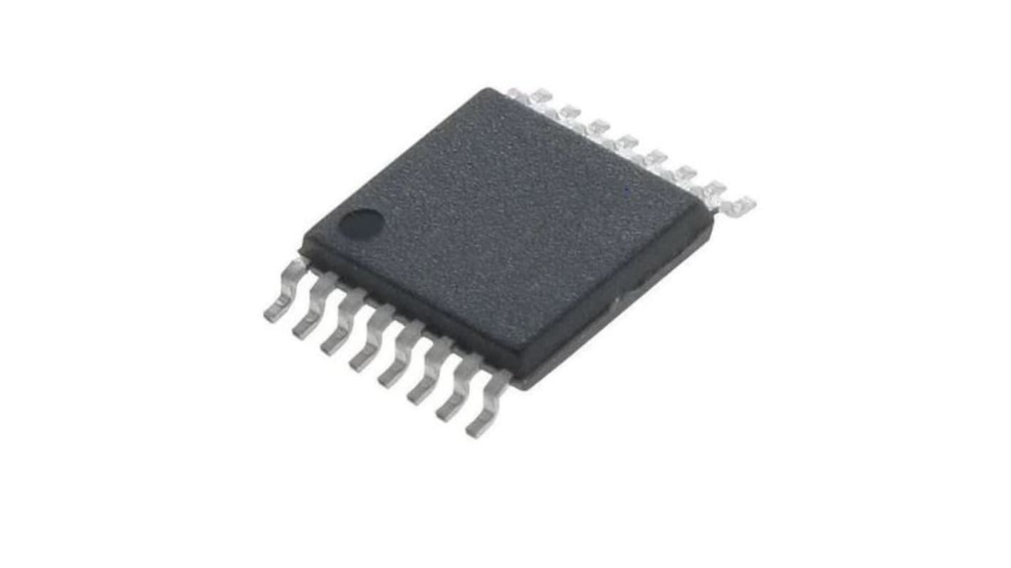
Renesas Electronics 85104AGILF Clock Buffer, 20-Pin 4 TSSOP
- RS 제품 번호:
- 216-6210
- 제조사 부품 번호:
- 85104AGILF
- 제조업체:
- Renesas Electronics

본 이미지는 참조용이오니 재확인이 필요하시면 문의해주세요.
현재 액세스할 수 없는 재고 정보
- RS 제품 번호:
- 216-6210
- 제조사 부품 번호:
- 85104AGILF
- 제조업체:
- Renesas Electronics
사양
참조 문서
제정법과 컴플라이언스
제품 세부 사항
제품 정보를 선택해 유사 제품을 찾기
모두 선택 | 제품 정보 | 값 |
|---|---|---|
| 브랜드 | Renesas Electronics | |
| Product Type | Clock Buffer | |
| Mount Type | Surface | |
| Package Type | TSSOP | |
| Pin Count | 20 | |
| Minimum Supply Voltage | 3V | |
| Maximum Supply Voltage | 3.3V | |
| Minimum Operating Temperature | -40°C | |
| Maximum Operating Temperature | 85°C | |
| Height | 1mm | |
| Standards/Approvals | No | |
| Length | 6.5mm | |
| Series | 85104A | |
| Automotive Standard | No | |
| Maximum Output Frequency | 700MHz | |
| 모두 선택 | ||
|---|---|---|
브랜드 Renesas Electronics | ||
Product Type Clock Buffer | ||
Mount Type Surface | ||
Package Type TSSOP | ||
Pin Count 20 | ||
Minimum Supply Voltage 3V | ||
Maximum Supply Voltage 3.3V | ||
Minimum Operating Temperature -40°C | ||
Maximum Operating Temperature 85°C | ||
Height 1mm | ||
Standards/Approvals No | ||
Length 6.5mm | ||
Series 85104A | ||
Automotive Standard No | ||
Maximum Output Frequency 700MHz | ||
The Renesas Electronics 85104I is a low skew, high performance 1-to-4 Differential/LVCMOS-to-0.7V HCSL Fanout Buffer. The 85104I has two selectable clock inputs. The CLK0, nCLK0 pair can accept most standard differential input levels. The single-ended CLK1 can accept LVCMOS or LVTTL input levels. The clock enable is internally synchronized to eliminate runt clock pulses on the outputs during asynchronous assertion/deassertion of the clock enable pin.
Four 0.7V differential HCSL outputs
Selectable differential CLK0, nCLK0 or LVCMOS inputs
CLK0, nCLK0 pair can accept the following differential
input levels: LVPECL, LVDS, LVHSTL, HCSL
CLK1 can accept the following input levels:
LVCMOS or LVTTL
Maximum output frequency: 500MHz
Translates any single-ended input signal to 3.3V
HCSL levels with resistor bias on nCLK input
Output skew: 100ps (maximum)
Part-to-part skew: 600ps (maximum)
Propagation delay: 3.2ns (maximum)
Additive phase jitter, RMS: 0.22ps (typical)
관련된 링크들
- Renesas Electronics 85104AGILF Clock Buffer, 20-Pin 4 TSSOP
- Renesas Electronics 85102AGILF Clock Buffer, 16-Pin 7 TSSOP
- Renesas Electronics 8305AGILF Clock Buffer, 16-Pin 4 TSSOP
- Renesas Electronics 9DB233AGILF Clock Buffer 20-Pin TSSOP
- Renesas Electronics 9DB833AGILF Clock Buffer 48-Pin TSSOP
- Renesas Electronics 9DB433AGILF Clock Buffer 28-Pin TSSOP
- Renesas Electronics 9DB633AGILF Clock Buffer 28-Pin TSSOP
- Renesas Electronics 853S014AGILF Buffer 20-Pin TSSOP