Infineon CY2309SXI-1H PLL Clock Buffer 16-Pin TSSOP
- RS 제품 번호:
- 194-9031
- 제조사 부품 번호:
- CY2309SXI-1H
- 제조업체:
- Infineon

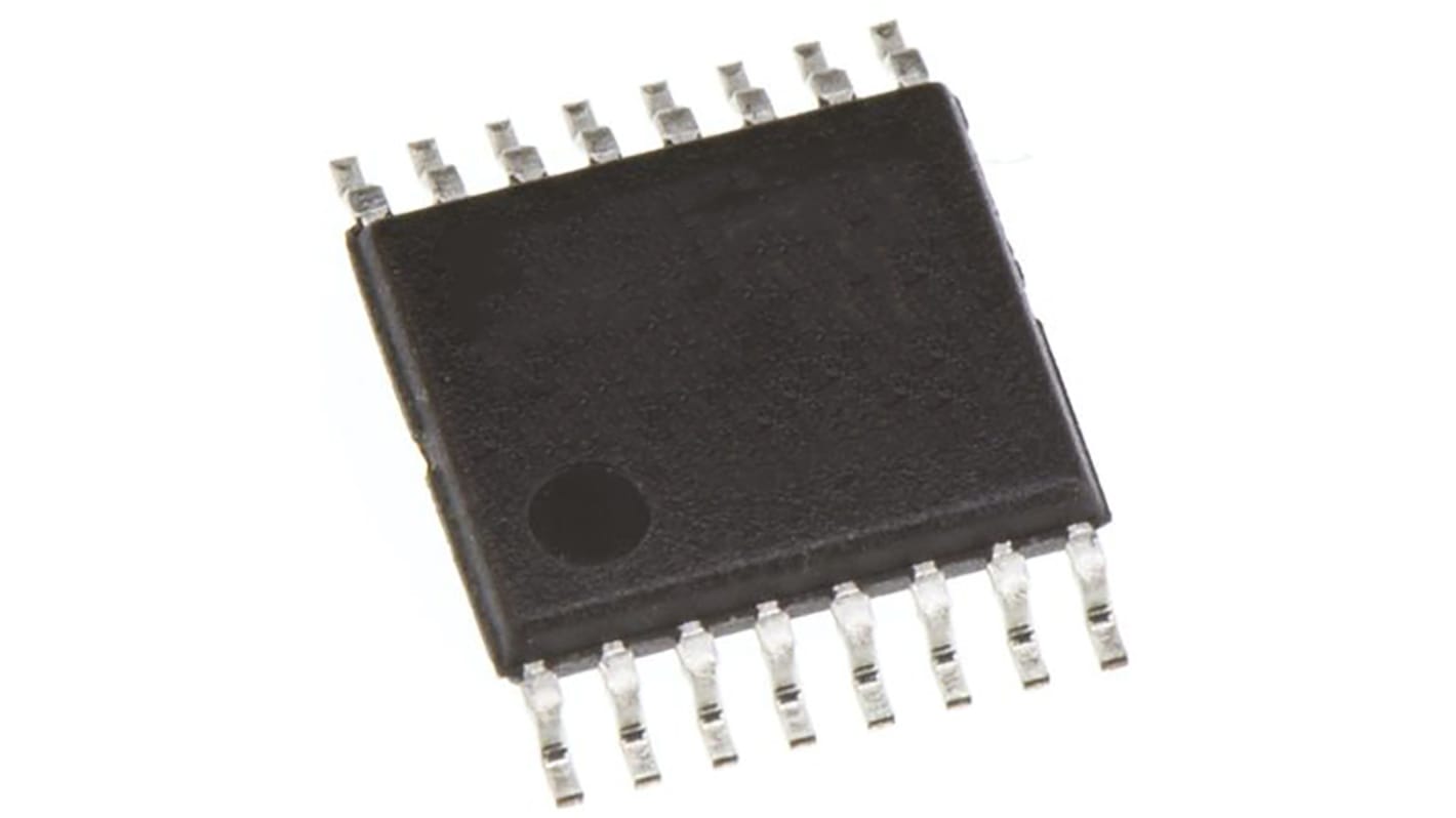
본 이미지는 참조용이오니 재확인이 필요하시면 문의해주세요.
현재 비가용
RS는 이 제품을 더 이상 판매하지 않습니다.
- RS 제품 번호:
- 194-9031
- 제조사 부품 번호:
- CY2309SXI-1H
- 제조업체:
- Infineon
사양
참조 문서
제정법과 컴플라이언스
제품 세부 사항
제품 정보를 선택해 유사 제품을 찾기
모두 선택 | 제품 정보 | 값 |
|---|---|---|
| 브랜드 | Infineon | |
| Product Type | PLL Clock Buffer | |
| Maximum Input Frequency | 133MHz | |
| Package Type | TSSOP | |
| Pin Count | 16 | |
| Minimum Operating Temperature | -40°C | |
| Maximum Operating Temperature | 85°C | |
| Length | 5.1mm | |
| Height | 0.95mm | |
| 모두 선택 | ||
|---|---|---|
브랜드 Infineon | ||
Product Type PLL Clock Buffer | ||
Maximum Input Frequency 133MHz | ||
Package Type TSSOP | ||
Pin Count 16 | ||
Minimum Operating Temperature -40°C | ||
Maximum Operating Temperature 85°C | ||
Length 5.1mm | ||
Height 0.95mm | ||
The CY2309 is a low-cost 3.3 V zero delay buffer designed to distribute high speed clocks and is available in a 16-pin SOIC or TSSOP package. The CY2305 is an 8-pin version of the CY2309. It accepts one reference input, and drives out five low skew clocks. The -1H versions of each device operate at up to 100-/133 MHz frequencies, and have higher drive than the -1 devices. All parts have on-chip PLLs which lock to an input clock on the REF pin. The PLL feedback is on-chip and is obtained from the CLKOUT pad. The CY2309 has two banks of four outputs each, which can be controlled by the select inputs. If all output clocks are not required, Bank B can be three-stated. The select inputs also allow the input clock to be directly applied to the outputs for chip and system testing purposes. The CY2305 and CY2309 PLLs enter a power-down mode when there are no rising edges on the REF input. In this state, the outputs are three-stated and the PLL is turned off, resulting in less than 25.0 μA current draw for these parts.
관련된 링크들
- Infineon CY2309SXI-1H PLL Clock Buffer 16-Pin TSSOP
- Infineon CY2308SXI-1 PLL Clock Buffer 16-Pin SOIC
- Infineon CY2302SXI-1 PLL Clock Buffer 8-Pin SOIC
- Infineon CY2308ZXI-1H PLL Clock Buffer 16-Pin TSSOP
- Infineon CY2305SXI-1 Clock Buffer 8-Pin SOIC
- Infineon CY2305SXI-1H Clock Buffer 8-Pin SOIC
- Infineon CY2304NZZXI-1 Clock Buffer 8-Pin TSSOP
- Infineon Clock Buffer 8-Pin SOIC