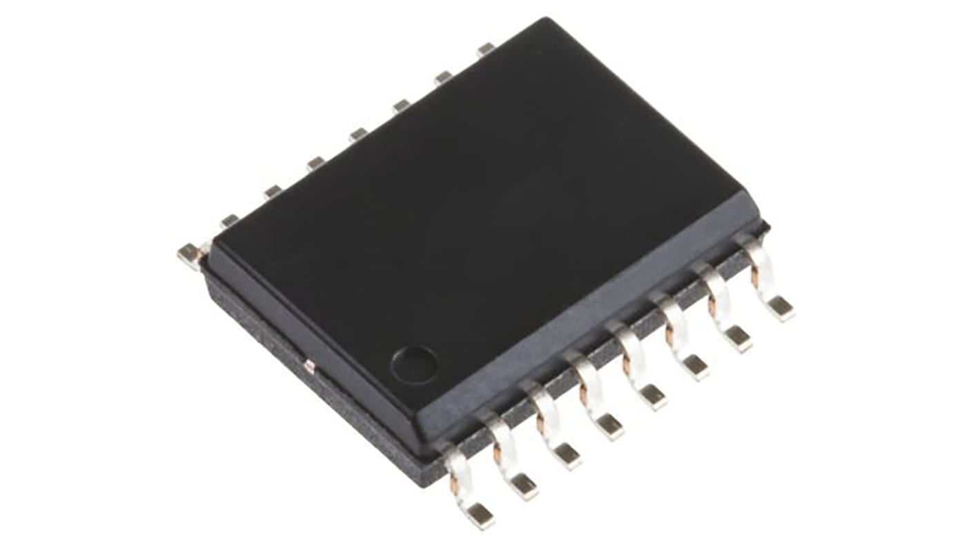
Infineon CY2308SXI-1 PLL Clock Buffer 16-Pin SOIC
- RS 제품 번호:
- 194-9014
- 제조사 부품 번호:
- CY2308SXI-1
- 제조업체:
- Infineon

본 이미지는 참조용이오니 재확인이 필요하시면 문의해주세요.
대량 구매 할인 기용 가능
Subtotal (1 unit)*
₩17,491.50
마지막 RS 재고
- 최종적인 2 개 unit(s)이 배송 준비 됨
수량 | 한팩당 |
|---|---|
| 1 - 11 | ₩17,491.50 |
| 12 - 23 | ₩17,043.00 |
| 24 + | ₩16,789.50 |
* 참고 가격: 실제 구매가격과 다를 수 있습니다
- RS 제품 번호:
- 194-9014
- 제조사 부품 번호:
- CY2308SXI-1
- 제조업체:
- Infineon
사양
참조 문서
제정법과 컴플라이언스
제품 세부 사항
제품 정보를 선택해 유사 제품을 찾기
모두 선택 | 제품 정보 | 값 |
|---|---|---|
| 브랜드 | Infineon | |
| Product Type | PLL Clock Buffer | |
| Maximum Input Frequency | 133.3MHz | |
| Package Type | SOIC | |
| Pin Count | 16 | |
| Minimum Operating Temperature | -40°C | |
| Maximum Operating Temperature | 85°C | |
| Length | 9.98mm | |
| Height | 1.47mm | |
| 모두 선택 | ||
|---|---|---|
브랜드 Infineon | ||
Product Type PLL Clock Buffer | ||
Maximum Input Frequency 133.3MHz | ||
Package Type SOIC | ||
Pin Count 16 | ||
Minimum Operating Temperature -40°C | ||
Maximum Operating Temperature 85°C | ||
Length 9.98mm | ||
Height 1.47mm | ||
The CY2308 is a 3.3 V Zero Delay Buffer designed to distribute high speed clocks in PC, workstation, datacom, telecom, and other high performance applications. The part has an on-chip PLL that locks to an input clock presented on the REF pin. The PLL feedback is driven from external FBK pin, so user has flexibility to choose any one of the outputs as feedback input and connect it to FBK pin. The input-to-output skew is less than 250 ps and output-to-output skew is less than 200 ps. The CY2308 has two banks of four outputs each that is controlled by the select inputs as shown in the table Select Input Decoding on page 3. If all output clocks are not required, Bank B is three-stated. The input clock is directly applied to the output for chip and system testing purposes by the select inputs. The CY2308 PLL enters a power down state when there are no rising edges on the REF input. In this mode, all outputs are three-stated and the PLL is turned off resulting in less than 25 μA of current draw.
관련된 링크들
- Infineon CY2308SXI-1 PLL Clock Buffer 16-Pin SOIC
- Infineon CY2302SXI-1 PLL Clock Buffer 8-Pin SOIC
- Infineon CY2309SXI-1H PLL Clock Buffer 16-Pin TSSOP
- Infineon CY2308ZXI-1H PLL Clock Buffer 16-Pin TSSOP
- Infineon CY2305SXI-1 Clock Buffer 8-Pin SOIC
- Infineon CY2305SXI-1H Clock Buffer 8-Pin SOIC
- Infineon Clock Buffer 8-Pin SOIC
- onsemi PLL Clock Buffer 8-Pin SOIC
