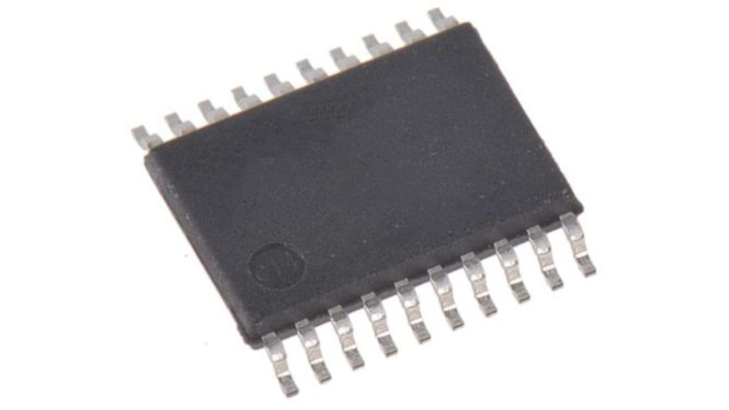
Renesas Electronics 9DB102BGILF, LVDS Buffer 2 TTL Buffer, 20-Pin TSSOP
- RS 제품 번호:
- 217-7928
- 제조사 부품 번호:
- 9DB102BGILF
- 제조업체:
- Renesas Electronics

본 이미지는 참조용이오니 재확인이 필요하시면 문의해주세요.
대량 구매 할인 기용 가능
View bulk pricing optionsSubtotal (1 tube of 74 units)*
₩395,160.00
일시적 품절
- 2027년 3월 15일 부터 배송
더 자세한 내용이 필요하신가요? 필요한 수량을 입력하고 '배송일 확인'을 클릭하면 더 많은 재고 및 배송 세부정보를 확인하실 수 있습니다.
수량 | 한팩당 | Per Tube* |
|---|---|---|
| 74 - 74 | ₩5,340.00 | ₩395,146.00 |
| 148 - 222 | ₩5,258.00 | ₩389,136.00 |
| 296 + | ₩5,142.00 | ₩380,538.00 |
* 참고 가격: 실제 구매가격과 다를 수 있습니다
- RS 제품 번호:
- 217-7928
- 제조사 부품 번호:
- 9DB102BGILF
- 제조업체:
- Renesas Electronics
사양
참조 문서
제정법과 컴플라이언스
제품 세부 사항
제품 정보를 선택해 유사 제품을 찾기
모두 선택 | 제품 정보 | 값 |
|---|---|---|
| 브랜드 | Renesas Electronics | |
| Product Type | LVDS Buffer | |
| Number of Drivers | 2 | |
| Input Type | TTL | |
| Sub Type | Buffer | |
| Output Type | Buffer | |
| Number of Elements per Chip | 2 | |
| Mount Type | Surface | |
| Package Type | TSSOP | |
| Pin Count | 20 | |
| Minimum Supply Voltage | 3V | |
| Maximum Supply Voltage | 3.3V | |
| Minimum Operating Temperature | -40°C | |
| ESD Protection | Yes | |
| Maximum Operating Temperature | 85°C | |
| Standards/Approvals | No | |
| Height | 1.05mm | |
| Length | 6.6mm | |
| Series | 9DB102 | |
| Automotive Standard | No | |
| 모두 선택 | ||
|---|---|---|
브랜드 Renesas Electronics | ||
Product Type LVDS Buffer | ||
Number of Drivers 2 | ||
Input Type TTL | ||
Sub Type Buffer | ||
Output Type Buffer | ||
Number of Elements per Chip 2 | ||
Mount Type Surface | ||
Package Type TSSOP | ||
Pin Count 20 | ||
Minimum Supply Voltage 3V | ||
Maximum Supply Voltage 3.3V | ||
Minimum Operating Temperature -40°C | ||
ESD Protection Yes | ||
Maximum Operating Temperature 85°C | ||
Standards/Approvals No | ||
Height 1.05mm | ||
Length 6.6mm | ||
Series 9DB102 | ||
Automotive Standard No | ||
The Renesas Electronics 9DB102 zero-delay buffer supports PCI Express clocking requirements. The 9DB102 is driven by a differential SRC output pair from an IDT CK409/CK410-compliant main clock generator such as the 952601 or 954101. It attenuates jitter on the input clock and has a selectable PLL Band Width to maximize performance in systems with or without Spread- Spectrum clocking.
2 - 0.7 V HCSL differential output pairs
Phase jitter: PCIe Gen2 < 3.1 ps rms
Phase jitter: PCIe Gen1 < 86 ps peak to peak
Supports zero delay buffer mode and fanout mode
Bandwidth programming available
33-110 MHz operation in PLL mode
10-110 MHz operation in Bypass mode
관련된 링크들
- Renesas Electronics 9DB102BGILF, LVDS Buffer 2 TTL Buffer, 20-Pin TSSOP
- Renesas Electronics 9DB403DGILFT, LVDS Buffer 4 TTL Buffer, 20-Pin TSSOP
- Renesas Electronics, LVDS Buffer 4 TTL Buffer, 20-Pin TSSOP
- Renesas Electronics 9DBL411BGILF PCIe Differential Buffer 20-Pin TSSOP
- Renesas Electronics 9DB102BGLF PCIe Differential Buffer 20-Pin TSSOP
- Renesas Electronics PCIe Differential Buffer 20-Pin TSSOP
- Renesas Electronics 9DB102BGLFT PLL Clock Buffer 20-Pin TSSOP-20
- Renesas Electronics 853S011BGILF Clock Buffer, 8-Pin 2 SOIC