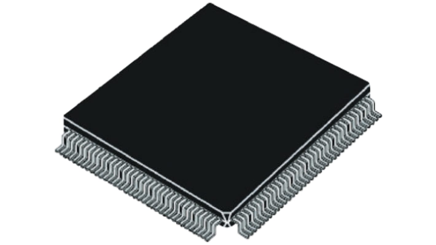
Lattice FPGA iCE40 3520 Cells, 80000 bit 440 Blocks, 144-Pin TQFP
- RS 제품 번호:
- 168-4222
- 제조사 부품 번호:
- ICE40HX4K-TQ144
- 제조업체:
- Lattice Semiconductor

본 이미지는 참조용이오니 재확인이 필요하시면 문의해주세요.
대량 구매 할인 기용 가능
View bulk pricing optionsSubtotal (1 tray of 60 units)*
₩1,089,360.00
재고있음
- 120 개 단위 배송 준비 완료
더 자세한 내용이 필요하신가요? 필요한 수량을 입력하고 '배송일 확인'을 클릭하면 더 많은 재고 및 배송 세부정보를 확인하실 수 있습니다.
수량 | 한팩당 | Per Tray* |
|---|---|---|
| 60 - 240 | ₩18,156.00 | ₩1,089,384.00 |
| 300 + | ₩17,792.00 | ₩1,067,580.00 |
* 참고 가격: 실제 구매가격과 다를 수 있습니다
- RS 제품 번호:
- 168-4222
- 제조사 부품 번호:
- ICE40HX4K-TQ144
- 제조업체:
- Lattice Semiconductor
사양
참조 문서
제정법과 컴플라이언스
제품 세부 사항
제품 정보를 선택해 유사 제품을 찾기
모두 선택 | 제품 정보 | 값 |
|---|---|---|
| 브랜드 | Lattice Semiconductor | |
| Product Type | FPGA | |
| Series | iCE40 | |
| Number of Logic Cells | 3520 | |
| Number of Logic Units | 440 | |
| Number of Registers | 3520 | |
| Mount Type | Surface | |
| Package Type | TQFP | |
| Minimum Supply Voltage | 1.14V | |
| Maximum Supply Voltage | 1.26V | |
| Pin Count | 144 | |
| Minimum Operating Temperature | -40°C | |
| Number of RAM Bits | 80000bit | |
| Maximum Operating Temperature | 85°C | |
| Length | 20mm | |
| Standards/Approvals | No | |
| Height | 1.45mm | |
| Automotive Standard | No | |
| 모두 선택 | ||
|---|---|---|
브랜드 Lattice Semiconductor | ||
Product Type FPGA | ||
Series iCE40 | ||
Number of Logic Cells 3520 | ||
Number of Logic Units 440 | ||
Number of Registers 3520 | ||
Mount Type Surface | ||
Package Type TQFP | ||
Minimum Supply Voltage 1.14V | ||
Maximum Supply Voltage 1.26V | ||
Pin Count 144 | ||
Minimum Operating Temperature -40°C | ||
Number of RAM Bits 80000bit | ||
Maximum Operating Temperature 85°C | ||
Length 20mm | ||
Standards/Approvals No | ||
Height 1.45mm | ||
Automotive Standard No | ||
- COO (Country of Origin):
- KR
Field Programmable Gate Arrays, Lattice Semiconductor
An FPGA is a semiconductor device consisting of a Matrix of Configurable Logic Blocks (CLBs) connected through programmable interconnects. The user determines these interconnections by programming SRAM. A CLB can be simple (AND, OR gates, etc) or complex (a Block of RAM). The FPGA allows changes to be MADE to a design even after the device is soldered into a PCB.
관련된 링크들
- Lattice FPGA iCE40HX4K-TQ144 iCE40 3520 Cells, 80000 bit 440 Blocks, 144-Pin TQFP
- Lattice FPGA iCE40 1280 Cells, 64000 bit 160 Blocks, 100-Pin VQFP
- Lattice FPGA iCE40HX1K-VQ100 iCE40 1280 Cells, 64000 bit 160 Blocks, 100-Pin VQFP
- Lattice FPGA iCE40 LP/HX 1280 Cells, 64 kB 160 Blocks, 49-Pin UCBGA
- Altera FPGA Cyclone II 4608 Cells, 4608 Blocks, 144-Pin TQFP
- Altera FPGA EP2C5T144C8N Cyclone II 4608 Cells, 4608 Blocks, 144-Pin TQFP
- Altera FPGA EP2C5T144I8N Cyclone II 4608 Cells, 4608 Blocks, 144-Pin TQFP
- Altera FPGA Cyclone IV E 6272 Cells, 6272 Gates, 276480 bit 392 Blocks, 144-Pin EQFP