FPGAs
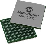
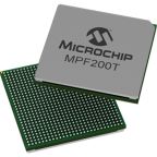
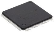
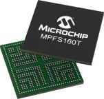
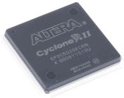
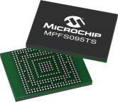
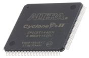
FPGA stands for Field Programmable Gate Array. They are small semiconductor logic chips are known as integrated circuits or ICs for short. FPGAs are built from one basic logic cell, duplicated hundreds of times.
What do they consist of?
They consist of a configurable logic block, programmable switch matrix, I/O blocks and Interconnects.
Configurable Logic Block
CLB consist of lookup tables (LUTs), flip flops and multiplexers. They are used to implement complex design functions and synchronise the code on the FPGA.
Programmable Switch Matrix
A programmable switch matrix (PSM) is used to control the interconnections between the configurable logic blocks and the input/output blocks. The programmable switch matrix connects each block according to the program code and has switch elements that have six pass transistors inside.
I/O Blocks
I/O blocks are pins that can be programmed as an input pin, output pins or both
Interconnects
Interconnects carry signals via wires to connect inputs and outputs to logic blocks.
How do FPGAs differ from CPLDs?
The main differences between the two devices is how they are made up. A CPLD device is very restricted in structure so they are less flexible. FPGAs on the other hand have a very high logic capacity and can be easily programmed to carry out any kind of digital function.
FPGA Applications
They are found in many applications such as radar systems, military hardware, medical devices and telecommunication technology. Their reprogrammable nature means FPGAs are suitable for a wide range of solutions. They can be any digital circuit, depending on the number of logic blocks it contains. Engineers often use FPGAs in prototype development and specially designed integrated circuits (ICs).
RS offer a range of high-quality devices from leading brands including Xilinx, Altera and Lattice Semiconductor. Our devices are available in industry standard package types, pin counts and mounting types to suit all your electronic design needs.
