Renesas Electronics Clock Buffer 20-Pin TSSOP
- RS 제품 번호:
- 254-4942
- 제조사 부품 번호:
- 5PB1110PGGI
- 제조업체:
- Renesas Electronics

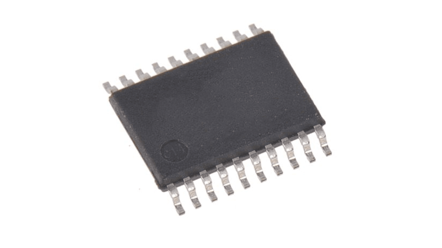
본 이미지는 참조용이오니 재확인이 필요하시면 문의해주세요.
현재 비가용
RS는 이 제품을 더 이상 판매하지 않습니다.
- RS 제품 번호:
- 254-4942
- 제조사 부품 번호:
- 5PB1110PGGI
- 제조업체:
- Renesas Electronics
사양
참조 문서
제정법과 컴플라이언스
제품 세부 사항
제품 정보를 선택해 유사 제품을 찾기
모두 선택 | 제품 정보 | 값 |
|---|---|---|
| 브랜드 | Renesas Electronics | |
| Product Type | Clock Buffer | |
| Maximum Input Frequency | 200MHz | |
| Mount Type | Surface | |
| Maximum Propagation Delay Time | 2.5ns | |
| Package Type | TSSOP | |
| Pin Count | 20 | |
| Minimum Supply Voltage | 1.71V | |
| Maximum Supply Voltage | 3.47V | |
| Minimum Operating Temperature | -40°C | |
| Maximum Operating Temperature | 105°C | |
| Height | 1.2mm | |
| Standards/Approvals | RoHS | |
| Series | 5PB11xx | |
| Length | 6.6mm | |
| Automotive Standard | No | |
| 모두 선택 | ||
|---|---|---|
브랜드 Renesas Electronics | ||
Product Type Clock Buffer | ||
Maximum Input Frequency 200MHz | ||
Mount Type Surface | ||
Maximum Propagation Delay Time 2.5ns | ||
Package Type TSSOP | ||
Pin Count 20 | ||
Minimum Supply Voltage 1.71V | ||
Maximum Supply Voltage 3.47V | ||
Minimum Operating Temperature -40°C | ||
Maximum Operating Temperature 105°C | ||
Height 1.2mm | ||
Standards/Approvals RoHS | ||
Series 5PB11xx | ||
Length 6.6mm | ||
Automotive Standard No | ||
The Renesas Electronics high-performance LVCMOS clock buffer has an additive phase jitter of 50 fs RMS. There are five different fan-out variations available that is 1:2 to 1:10. Its supports a synchronous glitch-free output enable (OE) function to eliminate any potential intermediate incorrect output clock cycles when enabling or disabling outputs. It can operate from a 1.8 V to 3.3 V supply.
High-performance 1:2, 1:4, 1:6, 1:8, 1:10 LVCMOS clock buffer
Very low pin-to-pin skew: < 50 ps
Very low additive jitter: < 50 fs
Supply voltage: 1.8 V to 3.3 V
3.3 V tolerant input clock
fMAX is 200 MHz
Integrated serial termination for 50 Ω channel
Packaged in 8-, 14-, 16-, 20-pin TSSOP and as small as 2 x 2 mm DFN and 3 x 3 mm VFQFPN packages
Industrial (-40°C to +85°C) and extended (-40°C to +105°C) temperature ranges
관련된 링크들
- Renesas Electronics 5PB1110PGGI Clock Buffer 20-Pin TSSOP
- Renesas Electronics 5PB1104PGGI8 Clock Buffer 8-Pin TSSOP
- Renesas Electronics 5PB1108PGGI8 Clock Buffer 16-Pin TSSOP-16
- Renesas Electronics 5PB1102PGGI Clock Buffer, 14-Pin 2 TSSOP
- Renesas Electronics 5PB1104PGGI Clock Buffer, 8-Pin 4 TSSOP
- Renesas Electronics 5PB1106PGGI Clock Buffer, 14-Pin 6 TSSOP
- Renesas Electronics High Performance Clock Buffer 24-Pin TSSOP
- Renesas Electronics 5PB1110NDGI Clock Buffer 20-Pin SOIC