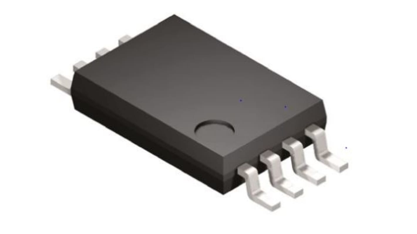
Renesas Electronics 5PB1102PGGI Clock Buffer, 14-Pin 2 TSSOP
- RS 제품 번호:
- 216-6166
- 제조사 부품 번호:
- 5PB1102PGGI
- 제조업체:
- Renesas Electronics

본 이미지는 참조용이오니 재확인이 필요하시면 문의해주세요.
대량 구매 할인 기용 가능
View bulk pricing optionsSubtotal (1 tube of 96 units)*
₩192,384.00
재고있음
- 추가로 2026년 7월 13일 부터 384 개 단위 배송
더 자세한 내용이 필요하신가요? 필요한 수량을 입력하고 '배송일 확인'을 클릭하면 더 많은 재고 및 배송 세부정보를 확인하실 수 있습니다.
수량 | 한팩당 | Per Tube* |
|---|---|---|
| 96 - 96 | ₩2,004.00 | ₩192,384.00 |
| 192 - 288 | ₩1,960.00 | ₩188,198.00 |
| 384 + | ₩1,920.00 | ₩184,416.00 |
* 참고 가격: 실제 구매가격과 다를 수 있습니다
- RS 제품 번호:
- 216-6166
- 제조사 부품 번호:
- 5PB1102PGGI
- 제조업체:
- Renesas Electronics
사양
참조 문서
제정법과 컴플라이언스
제품 세부 사항
제품 정보를 선택해 유사 제품을 찾기
모두 선택 | 제품 정보 | 값 |
|---|---|---|
| 브랜드 | Renesas Electronics | |
| Product Type | Clock Buffer | |
| Mount Type | Surface | |
| Package Type | TSSOP | |
| Minimum Supply Voltage | 1.8V | |
| Pin Count | 14 | |
| Maximum Supply Voltage | 3.3V | |
| Minimum Operating Temperature | -40°C | |
| Maximum Operating Temperature | 105°C | |
| Length | 3.1mm | |
| Standards/Approvals | No | |
| Height | 1mm | |
| Series | 5PB1102 | |
| Maximum Output Frequency | 200MHz | |
| Automotive Standard | No | |
| 모두 선택 | ||
|---|---|---|
브랜드 Renesas Electronics | ||
Product Type Clock Buffer | ||
Mount Type Surface | ||
Package Type TSSOP | ||
Minimum Supply Voltage 1.8V | ||
Pin Count 14 | ||
Maximum Supply Voltage 3.3V | ||
Minimum Operating Temperature -40°C | ||
Maximum Operating Temperature 105°C | ||
Length 3.1mm | ||
Standards/Approvals No | ||
Height 1mm | ||
Series 5PB1102 | ||
Maximum Output Frequency 200MHz | ||
Automotive Standard No | ||
The Renesas Electronics 5PB11xx is a high-performance LVCMOS clock buffer family of devices. It has an additive phase jitter of 50fs RMS. There are five different fan-out variations available: 1:2 to 1:10. The 5PB11xx supports a synchronous glitch-free output enable (OE) function to eliminate any potential intermediate incorrect output clock cycles when enabling or disabling outputs. It can operate from a 1.8V to 3.3V supply.
High-performance 1:2, 1:4, 1:6, 1:8, 1:10 LVCMOS clock buffer
Very low pin-to-pin skew: < 50ps
Very low additive jitter: < 50fs
Supply voltage: 1.8V to 3.3V
3.3V tolerant input clock
fMAX = 200MHz
Integrated serial termination for 50Ω channel
관련된 링크들
- Renesas Electronics 5PB1102PGGI Clock Buffer, 14-Pin 2 TSSOP
- Renesas Electronics 5PB1104PGGI Clock Buffer, 8-Pin 4 TSSOP
- Renesas Electronics 5PB1106PGGI Clock Buffer, 14-Pin 6 TSSOP
- Renesas Electronics 5PB1110PGGI Clock Buffer 20-Pin TSSOP
- Renesas Electronics 5PB1102CMGI8 Clock Buffer, 8-Pin TSSOP
- Renesas Electronics 5PB1104PGGI8 Clock Buffer 8-Pin TSSOP
- Renesas Electronics 5PB1108PGGI8 Clock Buffer 16-Pin TSSOP-16
- Renesas Electronics 5PB1102PGGK Clock Buffer 8-Pin TSSOP