Vishay EF Type N-Channel Power MOSFET, 6.5 A, 850 V Depletion, 3-Pin TO-220 SiHA17N80AEF-GE3
- RS 제품 번호:
- 239-8622
- 제조사 부품 번호:
- SiHA17N80AEF-GE3
- 제조업체:
- Vishay

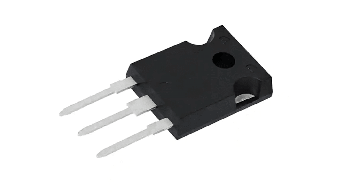
본 이미지는 참조용이오니 재확인이 필요하시면 문의해주세요.
대량 구매 할인 기용 가능
View bulk pricing optionsSubtotal (1 pack of 2 units)*
₩7,740.00
재고있음
- 추가로 2026년 7월 27일 부터 1,050 개 단위 배송
더 자세한 내용이 필요하신가요? 필요한 수량을 입력하고 '배송일 확인'을 클릭하면 더 많은 재고 및 배송 세부정보를 확인하실 수 있습니다.
수량 | 한팩당 | 한팩당* |
|---|---|---|
| 2 - 8 | ₩3,870.00 | ₩7,740.00 |
| 10 - 18 | ₩3,800.00 | ₩7,600.00 |
| 20 - 24 | ₩3,730.00 | ₩7,460.00 |
| 26 - 98 | ₩3,640.00 | ₩7,280.00 |
| 100 + | ₩3,570.00 | ₩7,140.00 |
* 참고 가격: 실제 구매가격과 다를 수 있습니다
- RS 제품 번호:
- 239-8622
- 제조사 부품 번호:
- SiHA17N80AEF-GE3
- 제조업체:
- Vishay
사양
참조 문서
제정법과 컴플라이언스
제품 세부 사항
제품 정보를 선택해 유사 제품을 찾기
모두 선택 | 제품 정보 | 값 |
|---|---|---|
| 브랜드 | Vishay | |
| Product Type | Power MOSFET | |
| Channel Type | Type N | |
| Maximum Continuous Drain Current Id | 6.5A | |
| Maximum Drain Source Voltage Vds | 850V | |
| Series | EF | |
| Package Type | TO-220 | |
| Mount Type | Surface | |
| Pin Count | 3 | |
| Maximum Drain Source Resistance Rds | 0.305Ω | |
| Channel Mode | Depletion | |
| Forward Voltage Vf | 1.2V | |
| Typical Gate Charge Qg @ Vgs | 63nC | |
| Maximum Power Dissipation Pd | 34W | |
| Maximum Gate Source Voltage Vgs | 30V | |
| Minimum Operating Temperature | -55°C | |
| Maximum Operating Temperature | +150°C | |
| Standards/Approvals | RoHS | |
| Automotive Standard | AEC-Q101 | |
| 모두 선택 | ||
|---|---|---|
브랜드 Vishay | ||
Product Type Power MOSFET | ||
Channel Type Type N | ||
Maximum Continuous Drain Current Id 6.5A | ||
Maximum Drain Source Voltage Vds 850V | ||
Series EF | ||
Package Type TO-220 | ||
Mount Type Surface | ||
Pin Count 3 | ||
Maximum Drain Source Resistance Rds 0.305Ω | ||
Channel Mode Depletion | ||
Forward Voltage Vf 1.2V | ||
Typical Gate Charge Qg @ Vgs 63nC | ||
Maximum Power Dissipation Pd 34W | ||
Maximum Gate Source Voltage Vgs 30V | ||
Minimum Operating Temperature -55°C | ||
Maximum Operating Temperature +150°C | ||
Standards/Approvals RoHS | ||
Automotive Standard AEC-Q101 | ||
Vishay Series EF Power MOSFET, 850V Drain Source Voltage, 6.5A Drain Current - SiHA17N80AEF-GE3
This power MOSFET is a high-voltage switching transistor designed for demanding electrical and automotive contexts. It operates as an N-channel depletion device in a through-hole TO-220 surface package, providing a Compact solution for power conversion and control where robust voltage handling and thermal margin are required.
Features and Benefits:
• 850V maximum drain-source voltage for high-voltage applications • 6.5A continuous drain current enabling sustained load handling • 0.305 Ω Rds minimises conduction losses under load • 34W power dissipation supports elevated thermal budgets • 63 nC typical gate charge for predictable switching control • ±150 °C/-55 °C operating range offers wide temperature endurance
Applications
• Suitable for high-voltage DC-DC converter stages in industrial systems • Ideal for inverter front ends and power-factor circuits • Used for switch-mode power supplies in automation equipment • Can be used for automotive power electronics meeting AEC‑Q101 criteria • Used with gate drivers requiring defined charge characteristics
What gate-voltage limits should be observed during design?
The device tolerates gate excursion up to 30 V
designs should ensure gate‑drive circuits remain within this limit to prevent gate-oxide stress.
How should thermal management be implemented for reliable operation?
Given a 34W dissipation rating, attach an appropriate heatsink to the TO‑220 tab and ensure sufficient airflow to maintain junction temperatures within safe bounds.
What considerations apply to switching losses and driver selection?
With a typical gate charge of 63 nC, choose a driver capable of sourcing and sinking the required Peak currents to achieve the desired rise/fall times while managing switching losses.
Is the device suitable for automotive qualification processes?
It conforms to AEC‑Q101 standards for automotive MOSFETs, making it appropriate for designs that require automotive‑grade components.
What electrical polarity and channel behaviour should designers expect?
The transistor is an N‑channel depletion device, so circuit topology must account for its channel mode when implementing normally‑on or normally‑off switching arrangements.
관련된 링크들
- Vishay EF Type N-Channel MOSFET, 6 A, 850 V Depletion, 3-Pin TO-220 SIHA15N80AEF-GE3
- Vishay EF Type N-Channel MOSFET, 7 A, 850 V Depletion, 3-Pin TO-220 SIHA21N80AEF-GE3
- Vishay EF Type N-Channel MOSFET, 6.5 A, 850 V Depletion, 3-Pin TO-220
- Vishay EF Type N-Channel MOSFET, 6 A, 850 V Depletion, 3-Pin TO-220
- Vishay EF Type N-Channel MOSFET, 7 A, 850 V Depletion, 3-Pin TO-220
- Vishay SiHA105N60EF Type N-Channel MOSFET, 29 A, 600 V Enhancement, 3-Pin TO-220 SIHA105N60EF-GE3
- Vishay SiHA125N60EF Type N-Channel MOSFET, 11 A, 600 V Enhancement, 3-Pin TO-220 SIHA125N60EF-GE3
- Vishay E Type N-Channel MOSFET, 15 A, 850 V Enhancement, 3-Pin TO-220 SiHP17N80AEF-GE3