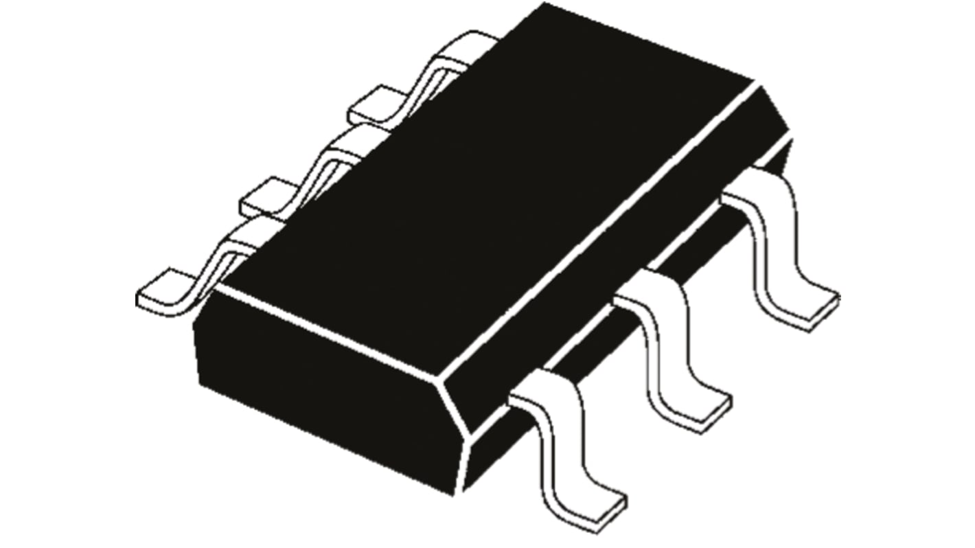
Vishay Isolated TrenchFET 2 Type P-Channel Power MOSFET, 1.1 A, 20 V Enhancement, 6-Pin SC-88
- RS 제품 번호:
- 145-2681
- 제조사 부품 번호:
- SI1967DH-T1-GE3
- 제조업체:
- Vishay

본 이미지는 참조용이오니 재확인이 필요하시면 문의해주세요.
대량 구매 할인 기용 가능
View bulk pricing optionsSubtotal (1 reel of 3000 units)*
₩936,000.00
일시적 품절
- 2026년 11월 16일 부터 배송
더 자세한 내용이 필요하신가요? 필요한 수량을 입력하고 '배송일 확인'을 클릭하면 더 많은 재고 및 배송 세부정보를 확인하실 수 있습니다.
수량 | 한팩당 | 릴당* |
|---|---|---|
| 3000 - 12000 | ₩312.00 | ₩933,600.00 |
| 15000 + | ₩304.00 | ₩915,000.00 |
* 참고 가격: 실제 구매가격과 다를 수 있습니다
- RS 제품 번호:
- 145-2681
- 제조사 부품 번호:
- SI1967DH-T1-GE3
- 제조업체:
- Vishay
사양
참조 문서
제정법과 컴플라이언스
제품 세부 사항
제품 정보를 선택해 유사 제품을 찾기
모두 선택 | 제품 정보 | 값 |
|---|---|---|
| 브랜드 | Vishay | |
| Channel Type | Type P | |
| Product Type | Power MOSFET | |
| Maximum Continuous Drain Current Id | 1.1A | |
| Maximum Drain Source Voltage Vds | 20V | |
| Series | TrenchFET | |
| Package Type | SC-88 | |
| Mount Type | Surface | |
| Pin Count | 6 | |
| Maximum Drain Source Resistance Rds | 790mΩ | |
| Channel Mode | Enhancement | |
| Typical Gate Charge Qg @ Vgs | 2.6nC | |
| Maximum Gate Source Voltage Vgs | 8V | |
| Minimum Operating Temperature | -55°C | |
| Maximum Power Dissipation Pd | 1.25W | |
| Transistor Configuration | Isolated | |
| Maximum Operating Temperature | 150°C | |
| Length | 2.2mm | |
| Width | 1.35mm | |
| Standards/Approvals | No | |
| Height | 1mm | |
| Number of Elements per Chip | 2 | |
| Automotive Standard | No | |
| 모두 선택 | ||
|---|---|---|
브랜드 Vishay | ||
Channel Type Type P | ||
Product Type Power MOSFET | ||
Maximum Continuous Drain Current Id 1.1A | ||
Maximum Drain Source Voltage Vds 20V | ||
Series TrenchFET | ||
Package Type SC-88 | ||
Mount Type Surface | ||
Pin Count 6 | ||
Maximum Drain Source Resistance Rds 790mΩ | ||
Channel Mode Enhancement | ||
Typical Gate Charge Qg @ Vgs 2.6nC | ||
Maximum Gate Source Voltage Vgs 8V | ||
Minimum Operating Temperature -55°C | ||
Maximum Power Dissipation Pd 1.25W | ||
Transistor Configuration Isolated | ||
Maximum Operating Temperature 150°C | ||
Length 2.2mm | ||
Width 1.35mm | ||
Standards/Approvals No | ||
Height 1mm | ||
Number of Elements per Chip 2 | ||
Automotive Standard No | ||
- COO (Country of Origin):
- CN
Vishay TrenchFET Series Power MOSFET, 20V Maximum Drain Source Voltage, 1.1A Maximum Continuous Drain Current - SI1967DH-T1-GE3
This power MOSFET is a P‑channel surface‑mount transistor designed for low‑voltage switching in Compact electronic systems. It operates as an enhancement‑mode device and is intended for board‑level power control where modest current handling and a small footprint are required.
Features and Benefits:
• 20V drain‑source rating enables low‑voltage system deployment • 1.1A continuous drain current supports light power switching • 790mΩ low Rds(on) reduces conduction losses during operation • 2.6nC typical gate charge permits Faster gate transitions • 1.25W power dissipation manages thermal load in small assemblies • Dual‑element isolated transistor allows paired switching arrangements
Applications
• Suitable for battery management and power rail switching in portable equipment • Ideal for load switching in industrial control modules • Used for reverse‑polarity protection in embedded systems • Can be used for signal level shifting in mixed‑voltage circuitry
What package should I plan for when designing the PCB?
The device is supplied in a 6‑pin SC‑88 SMD package that occupies a Compact footprint suitable for high‑density boards.
How does temperature affect operation limits?
The component is specified for operation between -55°C and 150°C, defining the allowable ambient and junction environments for reliable switching.
Can this component be used in automotive systems?
It is not classified to automotive standards, so suitability should be evaluated against vehicular qualification requirements before use.
What gate voltage range is permissible for control signals?
Gate drive must not exceed an 8V gate‑to‑source limit to avoid device overstress.
How many transistor elements are on the chip and what configuration are they?
The chip contains two isolated elements configured to enable paired or independent switching arrangements.
관련된 링크들
- Vishay Isolated TrenchFET 2 Type P-Channel Power MOSFET, 1.1 A, 20 V Enhancement, 6-Pin SC-88 SI1967DH-T1-GE3
- Vishay Isolated TrenchFET 2 Type N-Channel Power MOSFET, 1.3 A, 20 V Enhancement, 6-Pin SC-88
- Vishay Isolated TrenchFET 2 Type P, Type N-Channel MOSFET, 700 mA, 20 V Enhancement, 6-Pin SC-88
- Vishay Isolated TrenchFET 2 Type N-Channel Power MOSFET, 1.3 A, 20 V Enhancement, 6-Pin SC-88 SI1922EDH-T1-GE3
- Vishay Isolated TrenchFET 2 Type P, Type N-Channel MOSFET, 700 mA, 20 V Enhancement, 6-Pin SC-88 SI1553CDL-T1-GE3
- Vishay Isolated TrenchFET 2 Type P, Type N-Channel MOSFET, 300 mA, 60 V Enhancement, 6-Pin SC-89-6 SI1029X-T1-GE3
- Vishay Isolated TrenchFET 2 Type P, Type P-Channel MOSFET, 135 mA, 60 V Enhancement, 6-Pin SC-89-6 SI1025X-T1-GE3
- Vishay Isolated TrenchFET 2 Type P-Channel MOSFET, 8 A, 30 V Enhancement, 8-Pin SOIC