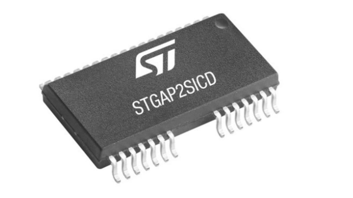
STMicroelectronics STGAP2SICDTR MOSFET Gate Driver, 4 A 36-Pin 5.5 V, SO-36W
- RS 제품 번호:
- 239-5534
- 제조사 부품 번호:
- STGAP2SICDTR
- 제조업체:
- STMicroelectronics

본 이미지는 참조용이오니 재확인이 필요하시면 문의해주세요.
대량 구매 할인 기용 가능
View bulk pricing optionsSubtotal (1 pack of 5 units)*
₩28,800.00
재고있음
- 추가로 2026년 7월 13일 부터 185 개 단위 배송
더 자세한 내용이 필요하신가요? 필요한 수량을 입력하고 '배송일 확인'을 클릭하면 더 많은 재고 및 배송 세부정보를 확인하실 수 있습니다.
수량 | 한팩당 | 한팩당* |
|---|---|---|
| 5 - 5 | ₩5,760.00 | ₩28,800.00 |
| 10 - 95 | ₩5,644.00 | ₩28,220.00 |
| 100 - 245 | ₩5,532.00 | ₩27,660.00 |
| 250 - 495 | ₩5,428.00 | ₩27,140.00 |
| 500 + | ₩5,316.00 | ₩26,580.00 |
* 참고 가격: 실제 구매가격과 다를 수 있습니다
- RS 제품 번호:
- 239-5534
- 제조사 부품 번호:
- STGAP2SICDTR
- 제조업체:
- STMicroelectronics
사양
참조 문서
제정법과 컴플라이언스
제품 세부 사항
제품 정보를 선택해 유사 제품을 찾기
모두 선택 | 제품 정보 | 값 |
|---|---|---|
| 브랜드 | STMicroelectronics | |
| Product Type | MOSFET | |
| Output Current | 4A | |
| Pin Count | 36 | |
| Fall Time | 30ns | |
| Package Type | SO-36W | |
| Driver Type | MOSFET | |
| Minimum Supply Voltage | 3.1V | |
| Maximum Supply Voltage | 5.5V | |
| Minimum Operating Temperature | -40°C | |
| Maximum Operating Temperature | 125°C | |
| Series | STGAP | |
| Standards/Approvals | No | |
| Automotive Standard | No | |
| 모두 선택 | ||
|---|---|---|
브랜드 STMicroelectronics | ||
Product Type MOSFET | ||
Output Current 4A | ||
Pin Count 36 | ||
Fall Time 30ns | ||
Package Type SO-36W | ||
Driver Type MOSFET | ||
Minimum Supply Voltage 3.1V | ||
Maximum Supply Voltage 5.5V | ||
Minimum Operating Temperature -40°C | ||
Maximum Operating Temperature 125°C | ||
Series STGAP | ||
Standards/Approvals No | ||
Automotive Standard No | ||
The STMicroelectronics STGAP2SiCD is a dual gate driver for SiC MOSFETs which provides galvanic isolation between each gate driving channel and the low voltage control and interface circuitry. The gate driver is characterized by 4 A current capability and rail-to-rail outputs, making it suitable for mid and high power applications such as power conversion and industrial motor drivers inverters. The separated output pins allow to independently optimize turn-on and turn-off by using dedicated gate resistors, while the Miller CLAMP function allows avoiding gate spikes during fast commutations in half-bridge topologies. The device integrates protection functions: dedicated SD and BRAKE pins are available, UVLO and thermal shutdown are included to easily design high reliability systems.
4 A Miller CLAMP
UVLO function
Configurable interlocking function
Dedicated SD and BRAKE pins
Gate driving voltage up to 26 V
3.3 V, 5 V TTL/CMOS inputs with hysteresis
Temperature shutdown protection
Standby function
6 kV galvanic isolation
Wide Body SO-36W
In half-bridge topologies the interlocking function prevents outputs from being high at the same time, avoiding shoot-through conditions in case of wrong logic input commands. The interlocking function can be disabled by a dedicated configuration pin, allowing independent and parallel operation of the two channels. The input to output propagation delay results are contained within 75 ns, providing high PWM control accuracy. A standby mode is available in order to reduce idle power consumption.
관련된 링크들
- STMicroelectronics MOSFET Gate Driver, 4 A 36-Pin 5.5 V, SO-36W
- STMicroelectronics STGAP2HDMTR MOSFET Gate Driver, 4 A 36-Pin 5.5 V, SO-36W
- STMicroelectronics STGAP2SICSNCTR MOSFET Gate Driver, 4 A 8-Pin 3.1 V, SO-8
- STMicroelectronics STGAP2SICS MOSFET Gate Driver 1, 4 A 8-Pin 5.5 V, SO-8
- STMicroelectronics STGAP2HSCMTR MOSFET Gate Driver 1, 4 A 8-Pin 5.5 V, SO-8
- STMicroelectronics STGAP2SICSNTR MOSFET Gate Driver 1, 4 A 8-Pin 5.5 V, SO-8
- STMicroelectronics STGAP2SICSANCTR MOSFET Gate Driver 1, 4 A 8-Pin 5.25 V, SO-8
- STMicroelectronics STGAP2SICSCTR MOSFET Gate Driver 1, 4 A 8-Pin 6.5 V, SO-8W