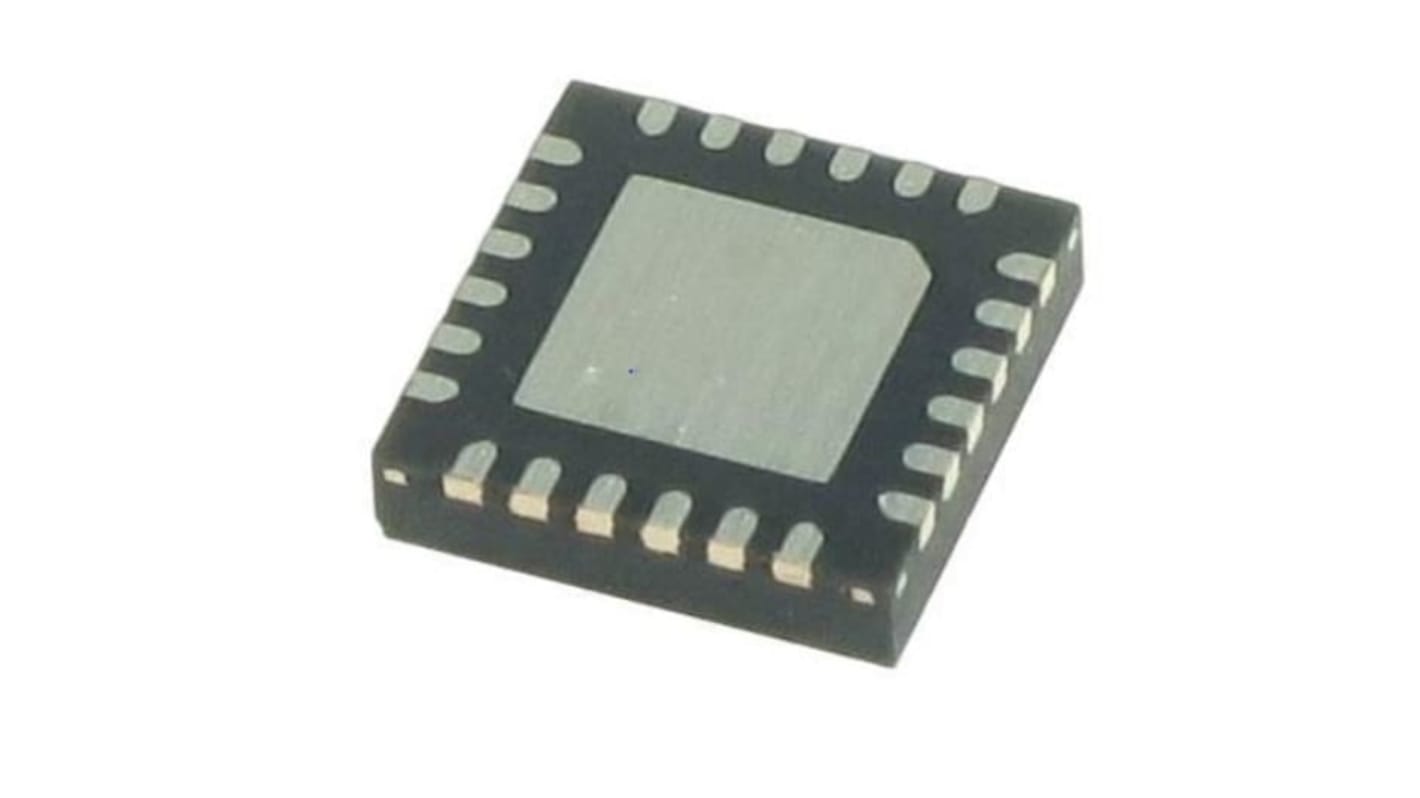
Renesas Electronics Clock Generator 24-Pin VFQFPN
- RS 제품 번호:
- 250-3449
- 제조사 부품 번호:
- 5P49V60A000NLG2
- 제조업체:
- Renesas Electronics

본 이미지는 참조용이오니 재확인이 필요하시면 문의해주세요.
현재 비가용
RS는 이 제품을 더 이상 판매하지 않습니다.
- RS 제품 번호:
- 250-3449
- 제조사 부품 번호:
- 5P49V60A000NLG2
- 제조업체:
- Renesas Electronics
사양
참조 문서
제정법과 컴플라이언스
제품 세부 사항
제품 정보를 선택해 유사 제품을 찾기
모두 선택 | 제품 정보 | 값 |
|---|---|---|
| 브랜드 | Renesas Electronics | |
| Product Type | Clock Generator | |
| Maximum Input Frequency | 40MHz | |
| Mount Type | Surface | |
| Package Type | VFQFPN | |
| Pin Count | 24 | |
| Minimum Supply Voltage | 1.71V | |
| Maximum Supply Voltage | 1.89V | |
| Minimum Operating Temperature | -40°C | |
| Maximum Operating Temperature | 105°C | |
| Standards/Approvals | RoHS | |
| Height | 1mm | |
| Series | 5P49V60 | |
| Length | 4mm | |
| Automotive Standard | No | |
| 모두 선택 | ||
|---|---|---|
브랜드 Renesas Electronics | ||
Product Type Clock Generator | ||
Maximum Input Frequency 40MHz | ||
Mount Type Surface | ||
Package Type VFQFPN | ||
Pin Count 24 | ||
Minimum Supply Voltage 1.71V | ||
Maximum Supply Voltage 1.89V | ||
Minimum Operating Temperature -40°C | ||
Maximum Operating Temperature 105°C | ||
Standards/Approvals RoHS | ||
Height 1mm | ||
Series 5P49V60 | ||
Length 4mm | ||
Automotive Standard No | ||
The Renesas Electronics programmable clock generator is intended for automotive applications. Configurations may be stored in on-chip One-Time Programmable (OTP) memory or changed using I2C interface. This is Renesas’ sixth generation of programmable clock technology (VersaClock 6E).The frequencies are generated from a single reference clock. The reference clock can come from one of the two redundant clock inputs. A glitch less manual switchover function allows one of the redundant clocks to be selected during normal operation. Two select pins allow up to four different configurations to be programmed and accessible using processor GPIOs or bootstrapping. The different selections may be used for different operating modes (full function, partial function, partial power-down), regional standards (US, Japan, Europe) or system production margin testing. The device may be configured to use one of two I2C addresses to allow multiple devices to be used in a system.
Flexible power rails available
High-performance with low phase noise PLL and less than 0.5ps RMS typical phase jitter on outputs
Four banks of internal OTP memory
In-system or factory programmable
2 select pins accessible with processor GPIOs or bootstrapping
I2C serial programming interface
0xD0 or 0xD4 I2C address options allows multiple devices configured in a same system
Reference LVCMOS output clock
Redundant clock inputs with manual switchover
Programmable output enable or power-down mode
4 x 4 mm 24-VFQFPN wet table flank package
AEC-Q100 qualified
-40° to +105°C (Grade 2) temperature operation
관련된 링크들
- Renesas Electronics 5P49V60A000NLG2 Clock Generator 24-Pin VFQFPN
- Renesas Electronics 5P49V6967A000NDGI Clock Generator 40-Pin VFQFPN
- Renesas Electronics 5P49V6901A000NLGI Clock Generator, 24-Pin VFQFPN
- Renesas Electronics 5P49V6965A000NLGI Clock Generator, 24-Pin 4 VFQFPN
- Renesas Electronics 5P49V5925B000NLGI PLL Clock Generator 24-Pin 3.465 V VFQFPN
- Renesas Electronics 5L1503-000NVGI Clock Generator, 10-Pin 3 VFQFPN
- Renesas Electronics 5X1503-000NLGI Clock Generator, 10-Pin 3 VFQFPN
- Renesas Electronics 9FGV0241AKILFT Clock Generator, 24-Pin VFQFPN