Infineon SRAM, CY7C1021D-10VXI- 1 MB
- RS 제품 번호:
- 194-8911
- 제조사 부품 번호:
- CY7C1021D-10VXI
- 제조업체:
- Infineon

현재 액세스할 수 없는 재고 정보
- RS 제품 번호:
- 194-8911
- 제조사 부품 번호:
- CY7C1021D-10VXI
- 제조업체:
- Infineon
사양
참조 문서
제정법과 컴플라이언스
제품 세부 사항
제품 정보를 선택해 유사 제품을 찾기
모두 선택 | 제품 정보 | 값 |
|---|---|---|
| 브랜드 | Infineon | |
| Memory Size | 1MB | |
| Product Type | SRAM | |
| Organisation | 64K x 16 bit | |
| Number of Words | 64K | |
| Number of Bits per Word | 16 | |
| Maximum Random Access Time | 10ns | |
| Minimum Supply Voltage | 5V | |
| Timing Type | Asynchronous | |
| Maximum Supply Voltage | 3.6V | |
| Mount Type | Through Hole | |
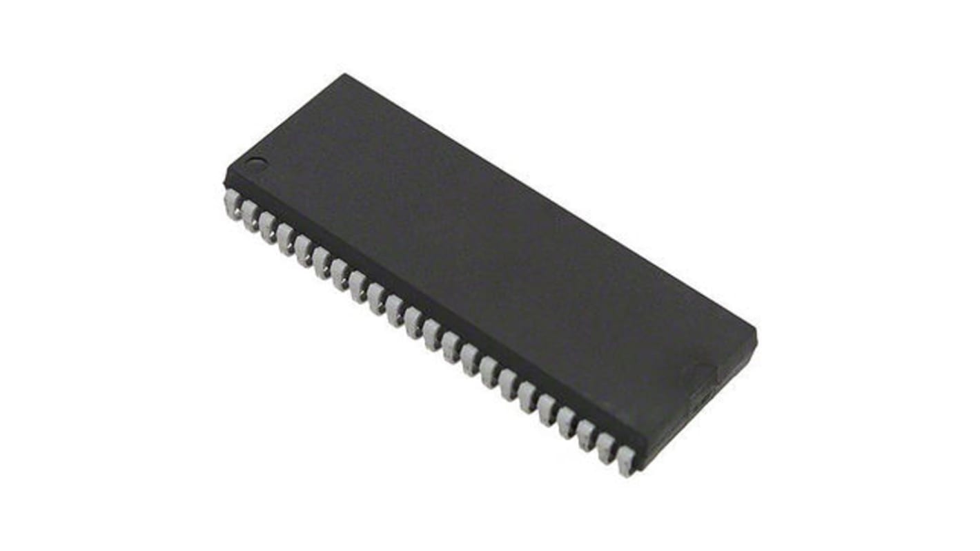
| Package Type | SOJ | |
| Minimum Operating Temperature | -40°C | |
| Maximum Operating Temperature | 85°C | |
| Pin Count | 44 | |
| Height | 3.05mm | |
| Length | 28.7mm | |
| Width | 10.29mm | |
| Standards/Approvals | RoHS | |
| 모두 선택 | ||
|---|---|---|
브랜드 Infineon | ||
Memory Size 1MB | ||
Product Type SRAM | ||
Organisation 64K x 16 bit | ||
Number of Words 64K | ||
Number of Bits per Word 16 | ||
Maximum Random Access Time 10ns | ||
Minimum Supply Voltage 5V | ||
Timing Type Asynchronous | ||
Maximum Supply Voltage 3.6V | ||
Mount Type Through Hole | ||
Package Type SOJ | ||
Minimum Operating Temperature -40°C | ||
Maximum Operating Temperature 85°C | ||
Pin Count 44 | ||
Height 3.05mm | ||
Length 28.7mm | ||
Width 10.29mm | ||
Standards/Approvals RoHS | ||
This device has an automatic power down feature that significantly reduces power consumption when deselected. The input and output pins (I/O0 through I/O15) are placed in a high impedance state when the device is deselected (CE HIGH), outputs are disabled (OE HIGH), BHE and BLE are disabled (BHE, BLE HIGH), or during a write operation (CE LOW and WE LOW). Write to the device by taking Chip Enable (CE) and Write Enable (WE) inputs LOW. If Byte Low Enable (BLE) is LOW, then data from I/O pins (I/O0 through I/O7), is written into the location specified on the address pins (A0 through A15). If Byte High Enable (BHE) is LOW, then data from I/O pins (I/O8 through I/O15) is written into the location specified on the address pins (A0 through A15). Read from the device by taking Chip Enable (CE) and Output Enable (OE) LOW while forcing the Write Enable (WE) HIGH. If Byte Low Enable (BLE) is LOW, then data from the memory location specified by the address pins appears on I/O0 to I/O7.
관련된 링크들
- Infineon SRAM, CY7C1021D-10VXI- 1 MB
- Infineon SRAM, CY7C109D-10VXI- 1 MB
- Infineon SRAM, CY7C1049GN-10VXI- 4 MB
- Infineon SRAM, CY7C1041G-10VXI- 4 MB
- Infineon SRAM, CY7C1049G30-10VXI- 4 MB
- Infineon SRAM, CY7C199D-10VXI- 256 kB
- Infineon SRAM, CY7C1021DV33-10ZSXIT- 1 MB
- Infineon SRAM, CY7C1021DV33-10ZSXI- 1 MB