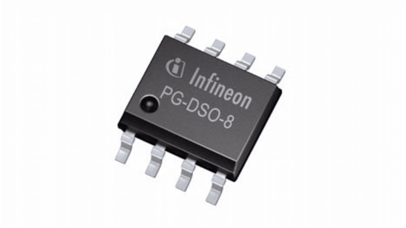
Infineon ITS4100SSJNXUMA1, 1High Side, High Side Power Switch IC 8-Pin, PG-DSO-8
- RS 제품 번호:
- 229-1862P
- 제조사 부품 번호:
- ITS4100SSJNXUMA1
- 제조업체:
- Infineon
대량 구매 할인 기용 가능
단가 개당(릴로 공급됨) 150pcs 이하는 STRIP 포장
₩1,904.29
4270 <재고있음> 5-9영업일내 홍콩 발송*
* 배송 날짜는 선택한 수량과 배송 주소에 따라 달라질 수 있습니다.
수량 | 한팩당 |
|---|---|
| 20 - 90 | ₩1,869.792 |
| 100 - 240 | ₩1,823.219 |
| 250 - 490 | ₩1,778.372 |
| 500 + | ₩1,733.525 |
- RS 제품 번호:
- 229-1862P
- 제조사 부품 번호:
- ITS4100SSJNXUMA1
- 제조업체:
- Infineon
MOTIX™ TLE9877QXW40 offers reliable solutions for automotive applications such as pumps and fans
The MOTIX™ TLE9877QXW40 is part of the MOTIX™ TLE987x product family. The MOTIX™ TLE9877QXW40 is a single chip 3-Phase motor driver that integrates the industry standard Arm® Cortex®-M3 core, enabling the implementation of advanced motor control algorithms such as field-oriented control. It includes six fully integrated NFET drivers optimized to drive a 3-Phase motor via six external power NFETs, a charge pump enabling low voltage operation and programmable current along with current slope control for optimized EMC behaviour. Its peripheral set includes a current sensor, a successive approximation ADC synchronized with the capture and compare unit for PWM control and 16-bit timers. A LIN transceiver is also integrated to enable communication to the device along with a number of general purpose I/Os. It includes an on-chip linear voltage regulator to supply external loads.
It is a highly integrated AEC-Q100 Grade 0 automotive qualified device enabling cost and space efficient solutions for mechatronic BLDC motor drive applications that are located under-the-hood such as pumps and fans.
It is a highly integrated AEC-Q100 Grade 0 automotive qualified device enabling cost and space efficient solutions for mechatronic BLDC motor drive applications that are located under-the-hood such as pumps and fans.
Summary of Features
•Six current programmable Drivers with charge pump for N-Channel MOSFET
•Integrated LIN transceiver compatible with LIN 2.2 and SAEJ2602
•Two Full duplex serial interface (UART) with LIN support
•Two Synchronous serial channel (SSC)
•On-chip OSC and PLL for clock generation
•One high voltage monitoring input with wake up functionality
•High speed Operational amplifier for motor current sensing via shunt
•Measurement unit:
8-bit ADC module with 10 multiplexed inputs
10-bit ADC module with 8 multiplexed inputs, 5 external Analog inputs
On chip temperature and battery voltage measurement unit
•Increased Temperature Shutdown supports operation up to Tjmax = 175 °C
•Independent Programmable window watchdog
•5V/1.5V Internal supplies
•External Supply (VDDEXT): 5V+/-2% @ 20mA
•Power saving modes:
MCU slow-down Mode
Sleep Mode
Stop Mode
Cyclic wake-up Sleep Mode
Features of the Microcontroller:
•32 bit Arm® Cortex®-M3 Core, up to 40 MHz clock frequency
•64 kByte flash memory for code and data
•32 kByte Boot ROM memory in code space (used for boot code and IP storage)
•6 kByte RAM memory
•Harvard architecture
•Thumb®-2 Instruction Set and hardware divide and multiplication unit
•Four 16-Bit timers
•Capture/compare unit for PWM signal generation (CCU6) with 2 x 16-bits timers
General Characteristics:
•Operating supply voltage Vs=5.5 to 28V, maximum rating 40V
• Extended operating range Vs=3.0 to 28V, MCU / Flash fully functional
•ESD performance :
up to 2kV / handling on all pins
4kV @ HV inputs
6kV @ LIN pin
•Overvoltage device clamp (load dump ruggedness) up to 40V
•Wide operating temperature range: Tj:-40°C up to 175°C
• Extended operating range Vs=3.0 to 28V, MCU / Flash fully functional
•ESD performance :
up to 2kV / handling on all pins
4kV @ HV inputs
6kV @ LIN pin
•Overvoltage device clamp (load dump ruggedness) up to 40V
•Wide operating temperature range: Tj:-40°C up to 175°C
For products that are Customized and under Non-cancellable & Non-returnable, Sales & Conditions apply.
속성 | 값 |
|---|---|
| Power Switch Type | High Side |
| Power Switch Topology | High Side |
| Switch On Resistance | 70MΩ |
| Number of Channels | 1 |
| Maximum Operating Supply Voltage | 40 V |
| Number of Outputs | 1 |
| Maximum Operating Current | 0.005A |
| Package Type | PG-DSO-8 |
| Pin Count | 8 |

