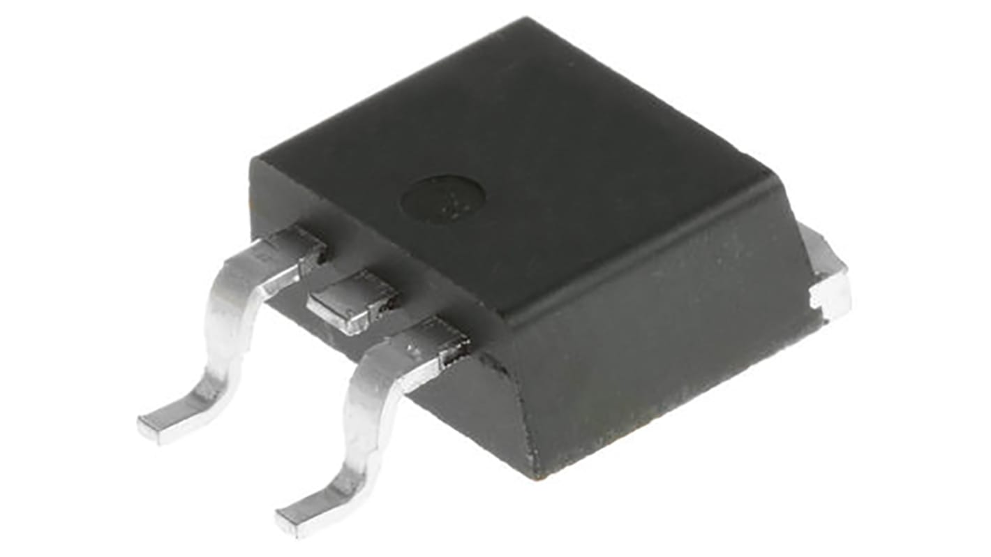
Infineon HEXFET Type N-Channel MOSFET, 33 A, 100 V Enhancement, 3-Pin TO-263 IRF540NSTRLPBF
- RS 제품 번호:
- 831-2831
- Distrelec 제품 번호:
- 304-44-447
- 제조사 부품 번호:
- IRF540NSTRLPBF
- 제조업체:
- Infineon

본 이미지는 참조용이오니 재확인이 필요하시면 문의해주세요.
대량 구매 할인 기용 가능
View bulk pricing optionsSubtotal (1 pack of 10 units)*
₩19,820.00
재고있음
- 10 개 단위 배송 준비 완료
- 추가로 2026년 7월 24일 부터 31,570 개 단위 배송
더 자세한 내용이 필요하신가요? 필요한 수량을 입력하고 '배송일 확인'을 클릭하면 더 많은 재고 및 배송 세부정보를 확인하실 수 있습니다.
수량 | 한팩당 | 한팩당* |
|---|---|---|
| 10 - 190 | ₩1,982.00 | ₩19,820.00 |
| 200 - 390 | ₩1,948.00 | ₩19,480.00 |
| 400 + | ₩1,914.00 | ₩19,140.00 |
* 참고 가격: 실제 구매가격과 다를 수 있습니다
- RS 제품 번호:
- 831-2831
- Distrelec 제품 번호:
- 304-44-447
- 제조사 부품 번호:
- IRF540NSTRLPBF
- 제조업체:
- Infineon
사양
참조 문서
제정법과 컴플라이언스
제품 세부 사항
제품 정보를 선택해 유사 제품을 찾기
모두 선택 | 제품 정보 | 값 |
|---|---|---|
| 브랜드 | Infineon | |
| Product Type | MOSFET | |
| Channel Type | Type N | |
| Maximum Continuous Drain Current Id | 33A | |
| Maximum Drain Source Voltage Vds | 100V | |
| Package Type | TO-263 | |
| Series | HEXFET | |
| Mount Type | Surface | |
| Pin Count | 3 | |
| Maximum Drain Source Resistance Rds | 44mΩ | |
| Channel Mode | Enhancement | |
| Maximum Power Dissipation Pd | 130W | |
| Typical Gate Charge Qg @ Vgs | 71nC | |
| Minimum Operating Temperature | -55°C | |
| Forward Voltage Vf | 1.2V | |
| Maximum Operating Temperature | 175°C | |
| Height | 4.83mm | |
| Length | 10.67mm | |
| Standards/Approvals | No | |
| Automotive Standard | No | |
| 모두 선택 | ||
|---|---|---|
브랜드 Infineon | ||
Product Type MOSFET | ||
Channel Type Type N | ||
Maximum Continuous Drain Current Id 33A | ||
Maximum Drain Source Voltage Vds 100V | ||
Package Type TO-263 | ||
Series HEXFET | ||
Mount Type Surface | ||
Pin Count 3 | ||
Maximum Drain Source Resistance Rds 44mΩ | ||
Channel Mode Enhancement | ||
Maximum Power Dissipation Pd 130W | ||
Typical Gate Charge Qg @ Vgs 71nC | ||
Minimum Operating Temperature -55°C | ||
Forward Voltage Vf 1.2V | ||
Maximum Operating Temperature 175°C | ||
Height 4.83mm | ||
Length 10.67mm | ||
Standards/Approvals No | ||
Automotive Standard No | ||
Infineon HEXFET Series MOSFET, 33A Maximum Continuous Drain Current, 130W Maximum Power Dissipation - IRF540NSTRLPBF
This high power MOSFET is designed for efficiency and reliability across a variety of applications. Featuring an N-channel configuration, it operates in enhancement mode with a maximum continuous drain current of 33A and a breakdown voltage of 100V. Its surface mount design allows for simple integration into printed circuit boards, enhancing versatility in modern applications.
Features & Benefits
• Low Rds(on) of 44mΩ improves circuit efficiency
• High power dissipation capability of 130W supports robust applications
• Fast switching speed minimises energy loss during operation
• Wide operating temperature range from -55°C to +175°C suits diverse environments
• Lead-free construction adheres to contemporary environmental standards
Applications
• Power management in automation systems
• High-efficiency power supplies for electronics
• Motor control in electrical engineering
• Renewable energy systems for effective energy conversion
What is the maximum gate-to-source voltage for this device?
The maximum gate-to-source voltage is ±20V, allowing for safe operation in typical circuits.
How does this device handle thermal management?
With a maximum power dissipation of 130W and a junction-to-case thermal resistance of 1.15°C/W, it effectively manages heat during operation.
What is the typical gate charge at 10V?
The typical gate charge at a gate-to-source voltage of 10V is 71 nC, ensuring quick response times in switching applications.
Can this device be mounted on standard PCBs?
Yes, it is designed in a D2PAK package, making it suitable for surface mount applications on standard PCB layouts.
What is the significance of the enhancement mode in this MOSFET?
The enhancement mode allows for greater control over the conduction state, providing improved performance in switching applications.
관련된 링크들
- Infineon HEXFET Type N-Channel MOSFET, 33 A, 100 V Enhancement, 3-Pin TO-263
- Infineon HEXFET Type N-Channel MOSFET, 33 A, 100 V Enhancement, 3-Pin TO-263 IRF540NSTRRPBF
- Infineon HEXFET Type N-Channel MOSFET, 17 A, 100 V Enhancement, 3-Pin TO-263 IRF530NSTRLPBF
- Infineon HEXFET Type P-Channel MOSFET, 23 A, 100 V Enhancement, 3-Pin TO-263 IRF9540NSTRLPBF
- Infineon HEXFET Type N-Channel MOSFET, 18 A, 200 V Enhancement, 3-Pin TO-263 IRF640NSTRLPBF
- Infineon HEXFET Type N-Channel MOSFET, 42 A, 100 V Enhancement, 3-Pin TO-263 IRF1310NSTRLPBF
- Infineon HEXFET Type P-Channel MOSFET, 14 A, 100 V Enhancement, 3-Pin TO-263 IRF9530NSTRLPBF
- Infineon HEXFET Type N-Channel MOSFET, 85 A, 55 V Enhancement, 3-Pin TO-263 IRF1010NSTRLPBF