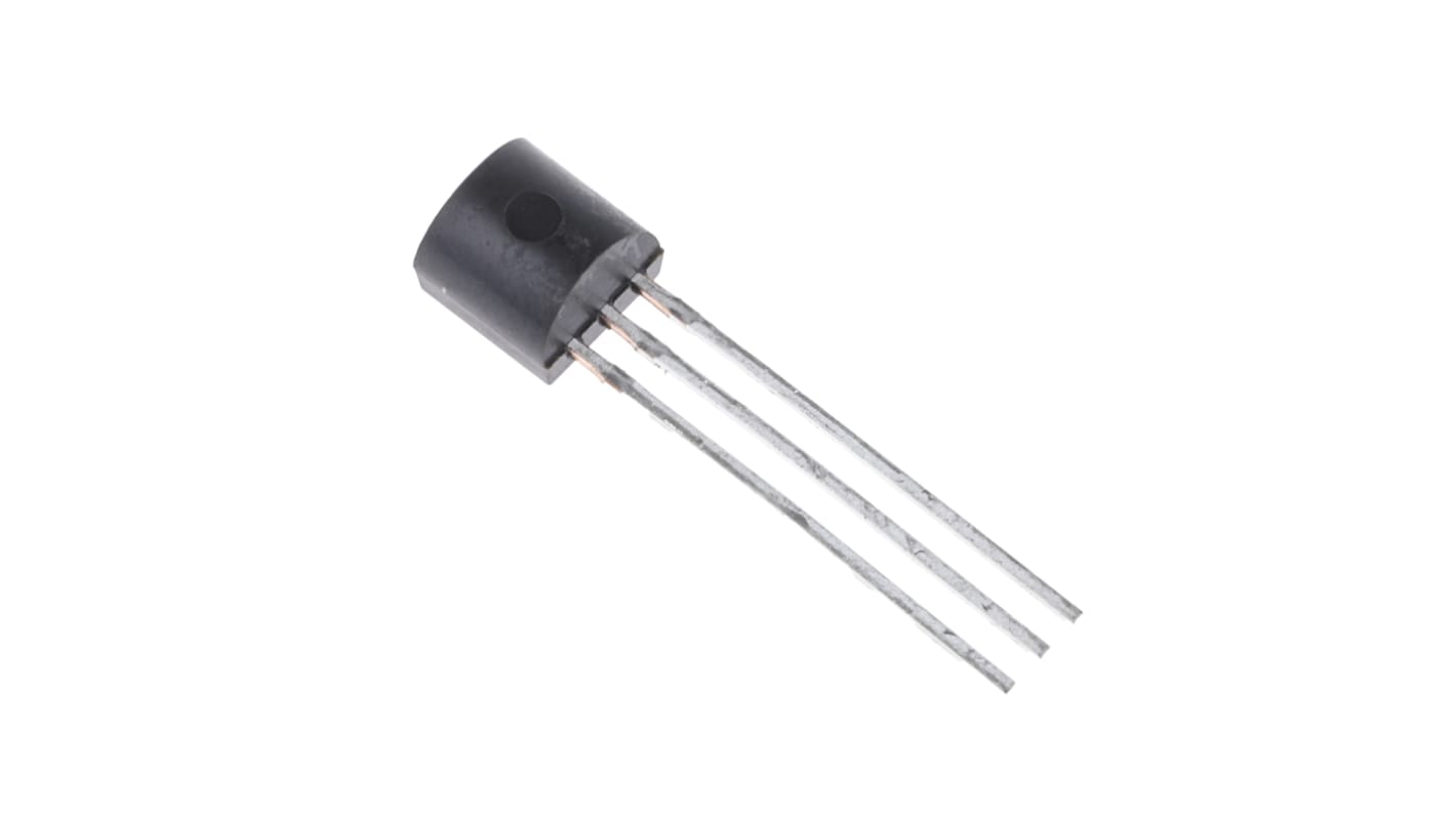
Microchip 2N7000 Type N-Channel MOSFET, 200 mA, 60 V Enhancement, 3-Pin TO-92 2N7000-G
- RS 제품 번호:
- 177-9760
- Distrelec 제품 번호:
- 304-38-475
- 제조사 부품 번호:
- 2N7000-G
- 제조업체:
- Microchip

본 이미지는 참조용이오니 재확인이 필요하시면 문의해주세요.
대량 구매 할인 기용 가능
View bulk pricing optionsSubtotal (1 pack of 25 units)*
₩16,900.00
재고있음
- 500 개 단위 배송 준비 완료
- 추가로 2026년 7월 22일 부터 2,600 개 단위 배송
더 자세한 내용이 필요하신가요? 필요한 수량을 입력하고 '배송일 확인'을 클릭하면 더 많은 재고 및 배송 세부정보를 확인하실 수 있습니다.
수량 | 한팩당 | 한팩당* |
|---|---|---|
| 25 - 225 | ₩676.00 | ₩16,880.00 |
| 250 + | ₩658.00 | ₩16,440.00 |
* 참고 가격: 실제 구매가격과 다를 수 있습니다
- RS 제품 번호:
- 177-9760
- Distrelec 제품 번호:
- 304-38-475
- 제조사 부품 번호:
- 2N7000-G
- 제조업체:
- Microchip
사양
참조 문서
제정법과 컴플라이언스
제품 세부 사항
제품 정보를 선택해 유사 제품을 찾기
모두 선택 | 제품 정보 | 값 |
|---|---|---|
| 브랜드 | Microchip | |
| Channel Type | Type N | |
| Product Type | MOSFET | |
| Maximum Continuous Drain Current Id | 200mA | |
| Maximum Drain Source Voltage Vds | 60V | |
| Package Type | TO-92 | |
| Series | 2N7000 | |
| Mount Type | Through Hole | |
| Pin Count | 3 | |
| Maximum Drain Source Resistance Rds | 5.3Ω | |
| Channel Mode | Enhancement | |
| Minimum Operating Temperature | -55°C | |
| Maximum Power Dissipation Pd | 1W | |
| Forward Voltage Vf | 0.85V | |
| Maximum Operating Temperature | 150°C | |
| Standards/Approvals | No | |
| Height | 5.33mm | |
| Length | 5.08mm | |
| Automotive Standard | No | |
| 모두 선택 | ||
|---|---|---|
브랜드 Microchip | ||
Channel Type Type N | ||
Product Type MOSFET | ||
Maximum Continuous Drain Current Id 200mA | ||
Maximum Drain Source Voltage Vds 60V | ||
Package Type TO-92 | ||
Series 2N7000 | ||
Mount Type Through Hole | ||
Pin Count 3 | ||
Maximum Drain Source Resistance Rds 5.3Ω | ||
Channel Mode Enhancement | ||
Minimum Operating Temperature -55°C | ||
Maximum Power Dissipation Pd 1W | ||
Forward Voltage Vf 0.85V | ||
Maximum Operating Temperature 150°C | ||
Standards/Approvals No | ||
Height 5.33mm | ||
Length 5.08mm | ||
Automotive Standard No | ||
- COO (Country of Origin):
- TW
Microchip Technology MOSFET
The Microchip Technology through-hole mount N-channel MOSFET is a new age product with a drain-source voltage of 60V and a maximum gate-source voltage of 30V. It has drain-source resistance of 5ohms at a gate-source voltage of 10V. It has continuous drain current of 200mA and maximum power dissipation of 1W. The minimum and a maximum driving voltage for this MOSFET is 4.5V and 10V respectively. The MOSFET is an enhancement mode (normally off) MOSFET that utilizes a vertical DMOS structure and well-proven, silicon gate manufacturing process. This combination produces a device with the power handling capabilities of bipolar transistors and the high input impedance and positive temperature coefficient inherent in MOS devices. A significant characteristic of all MOS structures, this device is free from thermal runaway and thermally induced secondary breakdown. This vertical DMOS FET has been optimized for lower switching and conduction losses. The MOSFET offers excellent efficiency along with a long and productive life without compromising performance or functionality.
Features and Benefits
• Ease of paralleling
• Excellent thermal stability
• Free from secondary breakdown
• High input impedance and high gain
• Integral source drain diode
• Low CISS and fast switching speeds
• Low power drive requirement
• Operating temperature ranges between -55°C and 150°C
Applications
• Amplifiers
• Converters
• Drivers: relays, hammers, solenoids, lamps, memories, displays, bipolar transistors, etc.
• Motor controls
• Power supply circuits
• Switches
Certifications
• ANSI/ESD S20.20:2014
• BS EN 61340-5-1:2007
• JEDEC
관련된 링크들
- Microchip 2N7000 Type N-Channel MOSFET, 200 mA, 60 V Enhancement, 3-Pin TO-92
- onsemi 2N7000 Type N-Channel MOSFET, 200 mA, 60 V Enhancement, 3-Pin TO-92 2N7000
- onsemi 2N7000 Type N-Channel MOSFET, 200 mA, 60 V Enhancement, 3-Pin TO-92 2N7000TA
- onsemi 2N7000 Type N-Channel MOSFET, 200 mA, 60 V Enhancement, 3-Pin TO-92 2N7000-D26Z
- onsemi 2N7000 Type N-Channel MOSFET, 200 mA, 60 V Enhancement, 3-Pin TO-92
- Microchip 2N7008 Type N-Channel MOSFET, 230 mA, 60 V Enhancement, 3-Pin TO-92
- Microchip Type N-Channel MOSFET, 3 A Enhancement, 3-Pin TO-92
- Microchip 2N7008 Type N-Channel MOSFET, 230 mA, 60 V Enhancement, 3-Pin TO-92 2N7008-G