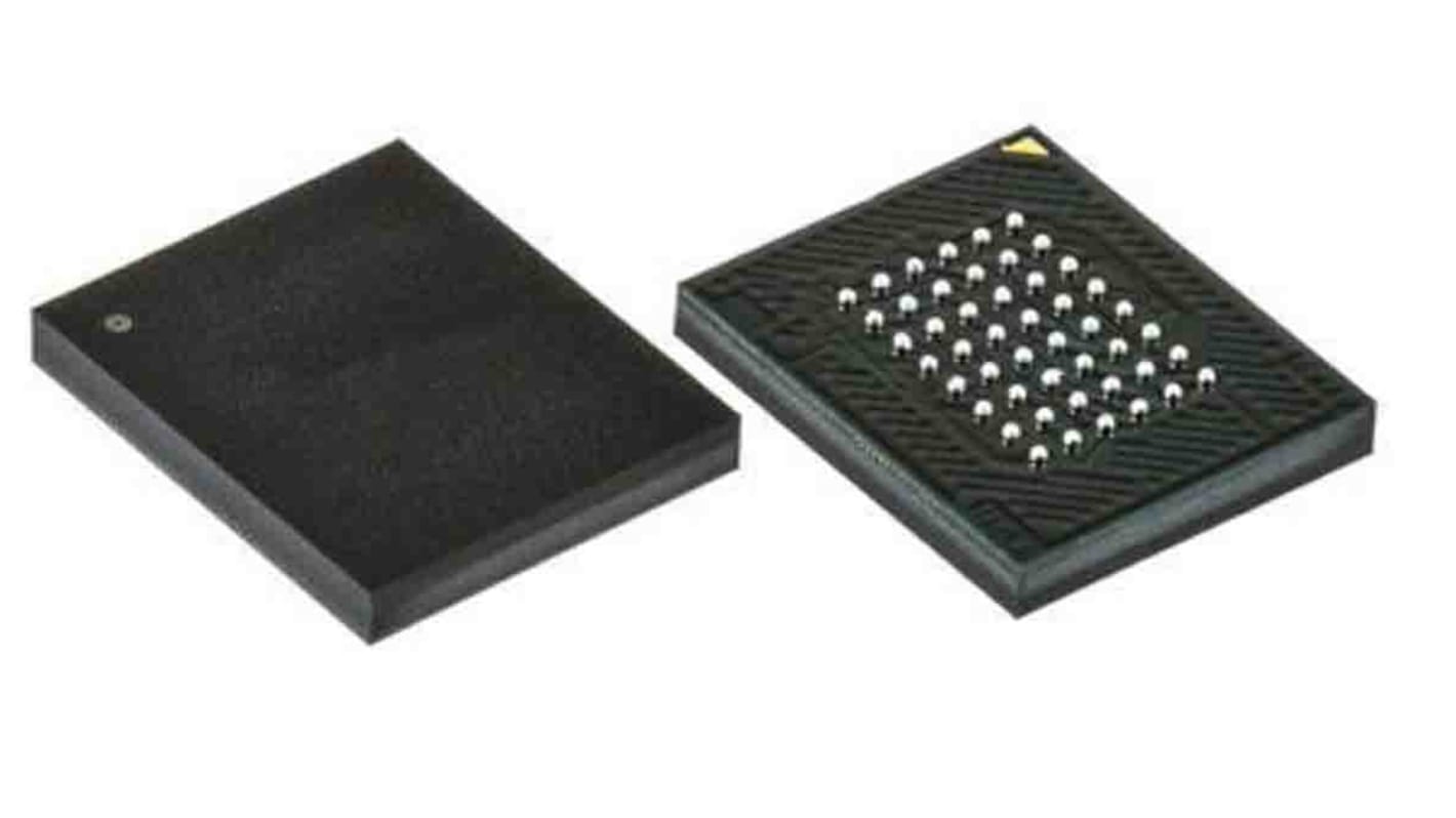
Infineon NOR 64 MB CFI Flash Memory 48-Pin BGA, S29GL064S70BHI030
- RS 제품 번호:
- 193-8826
- 제조사 부품 번호:
- S29GL064S70BHI030
- 제조업체:
- Infineon

본 이미지는 참조용이오니 재확인이 필요하시면 문의해주세요.
대량 구매 할인 기용 가능
View bulk pricing optionsSubtotal (1 pack of 5 units)*
₩34,760.00
재고있음
- 240 개 단위 배송 준비 완료
더 자세한 내용이 필요하신가요? 필요한 수량을 입력하고 '배송일 확인'을 클릭하면 더 많은 재고 및 배송 세부정보를 확인하실 수 있습니다.
수량 | 한팩당 | 한팩당* |
|---|---|---|
| 5 - 80 | ₩6,952.00 | ₩34,760.00 |
| 85 - 165 | ₩6,800.00 | ₩34,000.00 |
| 170 + | ₩6,652.00 | ₩33,260.00 |
* 참고 가격: 실제 구매가격과 다를 수 있습니다
- RS 제품 번호:
- 193-8826
- 제조사 부품 번호:
- S29GL064S70BHI030
- 제조업체:
- Infineon
사양
참조 문서
제정법과 컴플라이언스
제품 세부 사항
제품 정보를 선택해 유사 제품을 찾기
모두 선택 | 제품 정보 | 값 |
|---|---|---|
| 브랜드 | Infineon | |
| Memory Size | 64MB | |
| Product Type | Flash Memory | |
| Interface Type | CFI | |
| Package Type | BGA | |
| Pin Count | 48 | |
| Organisation | 8M x 8 bit | |
| Mount Type | Surface | |
| Cell Type | NOR | |
| Maximum Supply Voltage | 3.6V | |
| Minimum Supply Voltage | 2.7V | |
| Timing Type | Asynchronous | |
| Minimum Operating Temperature | -40°C | |
| Maximum Operating Temperature | 85°C | |
| Length | 8.15mm | |
| Width | 6.15mm | |
| Standards/Approvals | No | |
| Height | 0.84mm | |
| Number of Bits per Word | 8 | |
| Series | S29GL064S | |
| Maximum Random Access Time | 70ns | |
| Supply Current | 50mA | |
| Number of Words | 8K | |
| Automotive Standard | AEC-Q100 | |
| 모두 선택 | ||
|---|---|---|
브랜드 Infineon | ||
Memory Size 64MB | ||
Product Type Flash Memory | ||
Interface Type CFI | ||
Package Type BGA | ||
Pin Count 48 | ||
Organisation 8M x 8 bit | ||
Mount Type Surface | ||
Cell Type NOR | ||
Maximum Supply Voltage 3.6V | ||
Minimum Supply Voltage 2.7V | ||
Timing Type Asynchronous | ||
Minimum Operating Temperature -40°C | ||
Maximum Operating Temperature 85°C | ||
Length 8.15mm | ||
Width 6.15mm | ||
Standards/Approvals No | ||
Height 0.84mm | ||
Number of Bits per Word 8 | ||
Series S29GL064S | ||
Maximum Random Access Time 70ns | ||
Supply Current 50mA | ||
Number of Words 8K | ||
Automotive Standard AEC-Q100 | ||
The S29GL-S mid density family of devices are 3.0-volt single-power flash memory manufactured using 65 nm MirrorBit technology.
The S29GL064S is a 64-Mb device organized as 4,194,304 words or 8,388,608 bytes. Depending on the model number, the devices have 16bit wide data bus only, or a 16bit wide data bus that can also function as an 8bit wide data bus by using the BYTE# input.
The devices can be programmed either in the host system or in standard EPROM programmers. Access times as fast as 70 ns are available. Package offerings include 48pin TSOP, 56pin TSOP, 48-ball fine-pitch BGA, and 64-ball Fortified BGA, depending on model number. Each device has separate chip enable (CE#), write enable (WE#) and output enable (OE#) controls. Each device requires only a single 3.0-volt power supply for both read and write functions. In addition to a VCC input, a high-voltage accelerated program (ACC) feature is supported through increased voltage on the WP#/ACC or ACC input. This feature is intended to facilitate system production. Commands are written to the device using standard microprocessor write timing. Write cycles also internally latch addresses and data needed for the programming and erase operations.
The sector erase architecture allows memory sectors to be erased and reprogrammed without affecting the data contents of other sectors. The device is fully erased when shipped from the factory.
The Advanced Sector Protection features several levels of sector protection, which can disable both the program and erase operations in certain sectors.
관련된 링크들
- Infineon NOR 64 MB CFI Flash Memory 48-Pin BGA
- Infineon NOR 256 MB CFI Flash Memory 64-Pin BGA, S29GL256P11FFIV20
- Infineon NOR 256 MB CFI Flash Memory 64-Pin BGA
- Infineon NOR 512 MB CFI, SPI Flash Memory 24-Pin BGA
- Infineon NOR 512 MB CFI, SPI Flash Memory 24-Pin BGA, S25FL512SAGBHI310
- Infineon NOR 512 MB CFI, SPI Flash Memory 24-Pin BGA, S25FL512SAGBHID10
- Infineon 512 MB CFI Flash Memory 64-Pin BGA, S29GL512T11FHIV20
- Infineon NOR 1024 MB CFI Flash Memory 56-Pin TSOP, S29GL01GS11TFI010