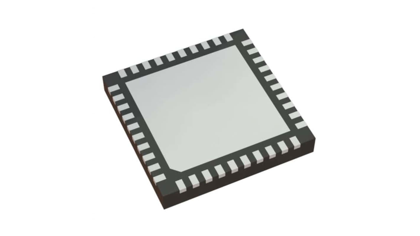
Renesas Electronics 8T49N242-999NLGI Clock Buffer 40-Pin VFQFN
- RS 제품 번호:
- 250-3483
- 제조사 부품 번호:
- 8T49N242-999NLGI
- 제조업체:
- Renesas Electronics

본 이미지는 참조용이오니 재확인이 필요하시면 문의해주세요.
현재 액세스할 수 없는 재고 정보
- RS 제품 번호:
- 250-3483
- 제조사 부품 번호:
- 8T49N242-999NLGI
- 제조업체:
- Renesas Electronics
사양
참조 문서
제정법과 컴플라이언스
제품 세부 사항
제품 정보를 선택해 유사 제품을 찾기
모두 선택 | 제품 정보 | 값 |
|---|---|---|
| 브랜드 | Renesas Electronics | |
| Product Type | Clock Buffer | |
| Maximum Input Frequency | 875MHz | |
| Mount Type | Surface | |
| Package Type | VFQFN | |
| Pin Count | 40 | |
| Minimum Supply Voltage | 3.14V | |
| Maximum Supply Voltage | 3.47V | |
| Minimum Operating Temperature | -40°C | |
| Maximum Operating Temperature | 85°C | |
| Length | 6mm | |
| Standards/Approvals | RoHS | |
| Series | 8T49N242 | |
| Height | 1mm | |
| Automotive Standard | No | |
| 모두 선택 | ||
|---|---|---|
브랜드 Renesas Electronics | ||
Product Type Clock Buffer | ||
Maximum Input Frequency 875MHz | ||
Mount Type Surface | ||
Package Type VFQFN | ||
Pin Count 40 | ||
Minimum Supply Voltage 3.14V | ||
Maximum Supply Voltage 3.47V | ||
Minimum Operating Temperature -40°C | ||
Maximum Operating Temperature 85°C | ||
Length 6mm | ||
Standards/Approvals RoHS | ||
Series 8T49N242 | ||
Height 1mm | ||
Automotive Standard No | ||
The Renesas Electronics frequency translator has one fractional-feedback PLL that can be used as a jitter attenuator and frequency translator. It is equipped with four integer output dividers, allowing the generation of up to four different output frequencies, ranging from 8kHz to 1GHz. These frequencies are completely independent of the input reference frequencies, and the crystal reference frequency. The outputs may select among LVPECL, LVDS, HCSL or LVCMOS output levels.
It accepts up to two differential or single-ended input clocks and a fundamental-mode crystal input
The internal PLL can lock to either of the input reference clocks or just to the crystal to behave as a frequency synthesizer
The device supports hitless reference switching between input clocks
The device monitors both input clocks for Loss of Signal and generates an alarm when an input clock failure is detected
The PLL has a register-selectable loop bandwidth from 0.2Hz to 6.4kHz
The device is programmable through an I2C interface
It also supports I2C master capability to allow the register configuration to be read from an external EEPROM
관련된 링크들
- Renesas Electronics 8T49N242-999NLGI Clock Buffer 40-Pin VFQFN
- Renesas Electronics 8T49N241-999NLGI Clock Generator, 40-Pin 4 VFQFN
- Renesas Electronics 5P49V5901B000NLGI Clock Generator 24-Pin VFQFN
- Renesas Electronics 8T49N241-998NLGI Clock Generator, 40-Pin 4 VFQFN
- Renesas Electronics 8T49N287A-998NLGI Clock Translator, 56-Pin 8 VFQFN-56
- Renesas Electronics 9DBL0455NLGI Clock Buffer 20-Pin VFQFPN
- Renesas Electronics 9FGV0231AKLF Clock Buffer 24-Pin VFQFN
- Renesas Electronics 5PB1102CMGK Clock Buffer 8-Pin VFQFN